- What is a multilayer PCB?
- The complete production process of multilayer PCB
- (1) the inner layer, mainly for the production of PCB circuit boards of the inner layer of the line; production process for.
- (2) internal inspection, mainly for board line detection and maintenance.
- (3) Press-fit; as the name implies, multiple inner laminates are pressed into one board.
- (4)Drilling
- (5) copper: the outer board has been drilled hole copper plating so that the board layers of the line conduct.
- (6) outer layer: the outer layer with the first step of the inner layer process is roughly the same; its purpose is to facilitate the subsequent process of making lines.
- (7) secondary copper and etching: secondary copper plating for etching.
- (8) solder resist: can protect the board from oxidation and other phenomena.
- (9) Text: printing text.
- (10) Surface treatment OSP
- (11)Forming
- (12) Flying probe test
- (13)FQC
- (14) Packaging, warehousing
- The development of multilayer printed circuit board applications.
- Contact Anpllopcb
What is a multilayer PCB?
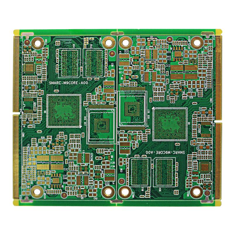
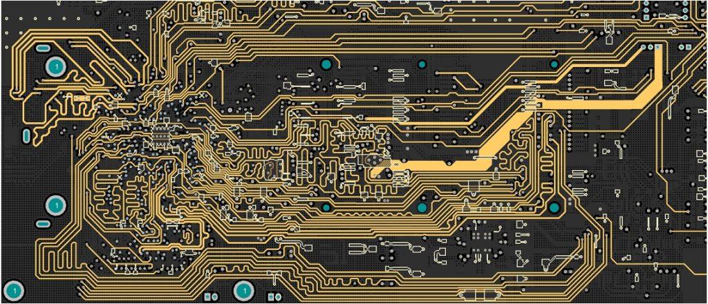
Multilayer PCB is a printed circuit board of alternating layers of conductive graphics and insulating materials laminated and bonded. The number of layers of conductive graphics is more than three, and the electrical interconnection between layers is achieved through metalized holes. If a double-sided printed circuit board for the inner layer, two single-sided printed circuit boards for the outer layer or two double-sided panels for the inner layer, two single-sided panels for the outer layer, through the positioning system and insulation bonding material laminated together, and the conductive graphics according to the design requirements for interconnection, it becomes a four-layer PCB, six-layer PCB, also known as multilayer PCB. More than 100 layers of practical multilayer PCB.
Multilayer printed circuit boards are generally manufactured with epoxy glass cloth laminated copper foil laminate; the manufacturing process is based on developing a double-sided printed circuit board process of plating over the holes. Its general process is to first etch the graphics of the inner board, after blackening treatment, according to the predetermined design to join the semi-curing sheet for lamination, and then put a copper foil on the upper and lower surfaces (also available in thin copper clad board, but the cost is higher), sent into the press after heating and pressing, to get a good preparation of the inner foil (also available in thin copper clad board, but the cost is higher), sent into the press after heating and pressing, to get a good preparation of the inner layer Graphic of a “double-sided copper-clad board,” and then according to the pre-designed positioning system, CNC drilling. After drilling the hole wall to be concave etching treatment, and removing the drilling dirt treatment, you can go on according to the double-sided plating hole printed circuit board.
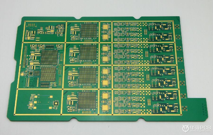
The complete production process of multilayer PCB
(1) the inner layer, mainly for the production of PCB circuit boards of the inner layer of the line; production process for.
1, the cutting board: the PCB substrate cut to production size.
2, pretreatment: clean the surface of the PCB substrate to remove surface contaminants
3, pressure film: the dry film is applied to the surface of the PCB substrate in preparation for subsequent image transfer.
4, exposure: use exposure equipment to expose the substrate with UV light to transfer the substrate’s image to the dry film.
5, DE: the exposure of the substrate after the development, etching, de-filming, and then complete the production of the inner layer of the board
(2) internal inspection, mainly for board line detection and maintenance.
1, AOI: AOI optical scanning, you can compare the image of the PCB board with the data of the good board that has been recorded to find the board image above the gap, depression, and other undesirable phenomena.
2, VRS: After the AOI detected bad image data to VRS, the relevant personnel to overhaul.
3, Patching: soldering the gold wire to the gap or depression to prevent electrical malpractice.
(3) Press-fit; as the name implies, multiple inner laminates are pressed into one board.
1, browning: browning increases the adhesion between the board and the resin and increases the copper surface’s wettability.
2, riveting: PP will be cut into small and normal sizes so that the inner layer of the board and the corresponding PP mou
3, Laminating and pressing, targeting, gong edge, and edge grinding.
(4)Drilling
1, drilling; according to the customer’s requirements, a drilling machine will be drilled out of different diameters and sizes so that the board between the holes for subsequent processing plug-ins also helps the board heat dissipation.
(5) copper: the outer board has been drilled hole copper plating so that the board layers of the line conduct.
1, deburring line: remove the burrs on the edge of the board holes to prevent poor copper plating.
2, deburring line: remove the slag inside the hole to increase adhesion during micro-etching.
3, a copper (pth): copper plating inside the hole to make the board all layers of the line conductivity while increasing the copper thickness.
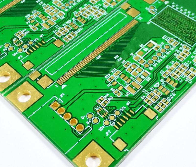
(6) outer layer: the outer layer with the first step of the inner layer process is roughly the same; its purpose is to facilitate the subsequent process of making lines.
1, pretreatment: clean the board’s surface by pickling, grinding, brushing, and drying to increase the dry film adhesion.
2, pressure film: the dry film on the surface of the PCB substrate in preparation for subsequent image transfer.
3, exposure: UV light irradiation so that the dry film on the board forms a polymerized and unpolymerized state.
4,Development: dissolve the dry film that has not been polymerized during the exposure process, leaving the pitch.
(7) secondary copper and etching: secondary copper plating for etching.
1, the second copper: plating graphics for the hole, is not covered with dry film to ferry the chemical copper; while further increasing the conductivity and copper thickness, and then after tinning to protect the integrity of the line and hole during etching.
2, SES: through de-filming, etching, stripping tin, and other process processing will be the outer dry film (wet film) attached to the area of the bottom copper etching, and the outer layer of the line to this production is complete.
(8) solder resist: can protect the board from oxidation and other phenomena.
1, pretreatment: acid washing, ultrasonic water washing, and other processes to remove the board oxide increase the roughness of the copper surface.
2, printing: the PCB board does not need to be covered with solder resist ink to play a protective, insulating role.
3, pre-baking: drying the solvent within the solder resist ink while hardening the ink for exposure.
4, exposure: curing solder resist ink by UV light irradiation, the formation of polymers through photosensitive polymerization.
5, development: removing the sodium carbonate solution within the unpolymerized ink.
6, Post-baking: complete hardening of the ink.
(9) Text: printing text.
1, acid washing: clean the surface of the plate to remove surface oxidation to enhance the adhesion of the printing ink.
2, text: printing text to facilitate the subsequent welding process.
(10) Surface treatment OSP
1, surface treatment OSP: the bare copper plate is to be welded on one side by coating treatment to form a layer of organic skin film to prevent rusting and oxidation.
(11)Forming
1, Forming: gong out the board appearance required by the customer to facilitate SMT placement and assembly.
(12) Flying probe test
1, flying probe test: test the board circuit to avoid short circuit board outflow.
(13)FQC
1, FQC: final inspection, full sampling inspection after completing all processes.
(14) Packaging, warehousing
1, Packaging, out of storage: the ready PCB board vacuum packaging, packing, and shipping, to complete the delivery.
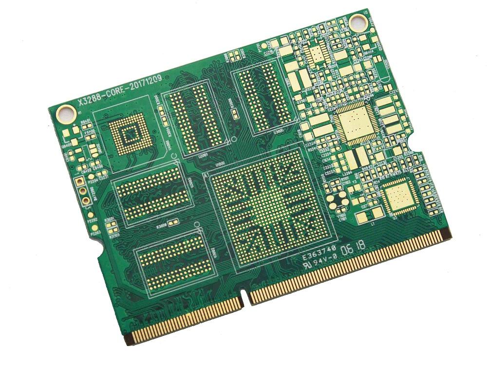
The development of multilayer printed circuit board applications.
Multilayer printed circuit board is the inevitable product of the development of electronic technology in the direction of high speed, multi-function, high capacity, and small volume. With the continuous development of electronics technology, especially large-scale and ultra-large-scale integrated circuits are widely used in-depth, multilayer printed circuit boards are rapid to the high-density, high-precision, high level of digital direction to mention the emergence of micro-fine lines, small aperture penetration, blind hole buried hole high board thickness aperture ratio and other technologies to meet the needs of the market as the computer and aerospace industry needs for high-speed circuits. Requirements to further improve the packaging density, coupled with the size of the separation of components and the rapid development of microelectronics, electronic equipment is to reduce the volume, the direction of mass reduction; single, double-sided printed circuit boards due to the limitations of the available space, it is impossible to achieve a further increase in assembly density. Therefore, it is necessary to consider using more layers than the double-sided printed circuit board. This creates the conditions for the emergence of multilayer printed circuit boards.
Contact Anpllopcb
Anpllopcb providing some of the most innovative printed circuit board technologies and highest quality standards in the industry. You can count on us to meet your needs, from the simplest boards to the most complex designs for small quantity and large scale production.

