- Five categories of PCB surface treatment processes
- PCB surface treatment process spray tin, dip silver and dip tin difference in which?
- PCB surface treatment process gold plating, gold immersion and nickel palladium gold difference in which?
- Summary
Five categories of PCB surface treatment processes
The most basic purpose of PCB surface treatment is to ensure good solderability or electrical properties. As copper is easily oxidized in the air, and the copper oxide layer has a great impact on the solder, if the copper layer is oxidized, it is easy to cause false solder; false solder serious will cause the pad and components can not be soldered. However, strong flux can be used to remove most of the copper oxide, but the residue of the strong flux itself will also bring corrosion to the product. Therefore, the industry’s common way to deal with the PCB manufacturing process is to add a process, that is, in the pad surface coating (plating) on a layer of material to protect the pad from oxidation.
The current PCB surface treatment process are: spray tin (Hot Air Solder Leveling, HASL hot air levelling), OSP (anti-oxidation), full board plating nickel gold, pink gold, sink tin, sink silver, chemical nickel palladium gold, electroplated hard gold, some special applications will have some special PCB surface treatment process. The following is a brief introduction.
(1) hot air levelling (tin spraying)
Hot air levelling, also known as hot air solder levelling (commonly known as spray tin), is coated with molten tin (lead) solder on the surface of the PCB and heated compressed air levelling (blowing) process to form a layer of both copper oxidation resistance and can provide a good solderable coating. Hot air levelling of solder and copper in combination with the formation of copper-tin intermetallic compounds. For hot air levelling to sink in the molten solder, air knife in the solder solidification before blowing flat liquid solder to minimize the copper surface solder bending moon shape and prevent solder bridging. There are two types of hot air levelling: vertical and horizontal. The horizontal type is generally better, with more uniform plating and easier-to-automate production.
① The advantages of the HASL process are lower prices and better soldering performance.
②The disadvantage of the HASL process is that it is not suitable for soldering fine pitch pins and components that are too small because the surface flatness of the spray tin plate is poor. It is easy to produce tin beads (solder beads) during the subsequent assembly process, making it easier to cause short circuits for fine-pitch pins (fine-pitch) components.
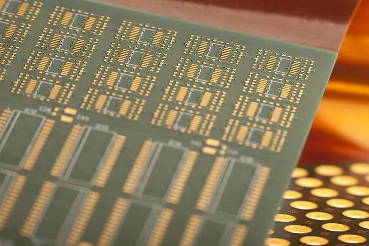
(2) Organic solderable flux (OSP) process
The organic Solderability Protectant (OSP) process is a PCB copper foil surface treatment to meet the requirements of the RoHS Directive process. Worldwide, 25% to 30% of PCBs use the OSP process, and the proportion continues to rise. osp process can be used in low-tech PCBs and can also be used in high-tech PCBs, such as single-sided TV PCBs and high-density chip packaging PCB. for PCBs containing BGA devices, OSP applications are also more. In fact, for applications with no functional requirement for surface connection or limited storage period, the OSP process will be the ideal surface treatment process.
① The OSP process’s advantages are simple, very flat surface, and suitable for lead-free soldering and SMT.
② The disadvantages of the OSP process are: that nitrogen is required for soldering, the number of reflow soldering is limited (multiple soldering will lead to film destruction, 2 times is no problem), not suitable for crimping technology, not suitable for rework and high storage condition requirement.
(3) Full-board nickel gold plating
Full-board nickel gold plating is a nickel layer on the PCB surface conductors. Before plating a layer of gold, nickel plating mainly prevents the diffusion of gold and copper. There are two main types of electroplated nickel gold: soft gold plating (pure gold, the surface does not look bright) and hard gold plating (smooth and hard surface, wear-resistant, containing other elements such as cobalt, the surface looks brighter). Soft gold is mainly used for chip packaging when playing gold wire; hard gold is mainly used in the non-solder at the electrical interconnection.
① The advantages of the gold plating process are longer storage time (>12 months), suitable for contact switch design and gold wire bonding, and suitability for electrical testing.
② The disadvantages of the gold plating process are higher cost, thicker gold and poor consistency of the gold layer thickness, the soldering process, and maybe too thick gold and lead to brittle solder joints, affecting the strength.
(4) chemical nickel/immersion gold (ENIG)
Electroless nickel/immersion gold also called sink gold, is wrapped in a thick layer of the copper surface, an electrical good nickel alloy, which can be long-term protection of PCB. ENIG has other surface treatment processes that do not have the tolerance of the environment; in addition to sinking, gold can also prevent the dissolution of copper, which will benefit the lead-free assembly.
①The advantages of the ENIG process are: it not easy to oxidize; it can be stored for a long time; the surface is flat, suitable for soldering fine gap pins and components with small solder joints; it can withstand multiple reflows, suitable for rework, and suitable for use as a substrate for COB (Chip On Board) hitting the line.
② The disadvantages of the ENIG process are: higher cost, poorer soldering strength, easy-to-produce black disc problems, nickel layer will gradually oxidize over time and poor long-term reliability.
(5) Other surface treatment processes
Other surface treatment processes include the sink tin process, sink silver process, chemical nickel palladium gold, electroplating hard gold, Etc.
① Sink tin process: Due to the good compatibility with the solder, it has good solderability, while its excellent flatness is suitable for lead-free soldering and crimping; the disadvantage is that it is not resistant to storage. N2 best protects the soldering process, and it is easy to produce “tin whiskers”.
② Silver sink process: between the organic coating and chemical nickel / sink gold, the process is relatively simple; even if exposed to heat, humidity and pollution environment, silver can still maintain good solderability; the disadvantage is that it does not have chemical nickel / sink gold with good physical strength, storage conditions require high, easy to contaminate, easy to oxidation, while the solder strength is not good, easy to micro-hole problems.
③ Chemical nickel palladium gold: compared with sunken gold between nickel and gold with an additional layer of palladium, thus having better corrosion resistance, strong resistance to environmental attack, suitable for long time storage, suitable for lead-free soldering, thick boards and switch contact design, Etc.
④ Hard gold plating: commonly used in electrical connector “contact pairs” with high requirements for wear resistance.
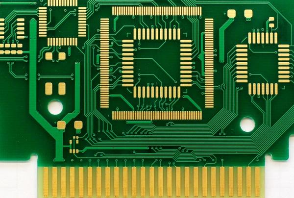
PCB surface treatment process spray tin, dip silver and dip tin difference in which?
In the PCB surface treatment process, many people are often confused with “spray tin”, “immersion silver”, and “immersion tin” and think they are similar. So, are the PCB board surface treatment process “spray tin”, “immersion silver”, and “immersion tin” where the difference is?
1, spray tin
Silver-coloured plate called spray tin plate. Spraying a layer of tin in the outer layer of copper lines helps to solder; however, it does not provide long-lasting contact reliability like gold. Long-term use is prone to oxidation and rust, resulting in poor contact.
Advantages: Lower price and good soldering performance.
Disadvantages: The surface flatness of the sprayed tin plate is poor, and it is not suitable for soldering fine gap pins and components that are too small. It is easy to produce tin beads in PCB processing, and it is easy to cause short circuits to fine-gap pins. When used in a double-sided SMT process, it is very easy to melt the spray tin again and produce tin beads or spherical tin dots, resulting in a more uneven surface and thus affecting the soldering problem.
2、Silver dip
The immersion of the silver process is simpler and faster. Immersion of silver is a replacement reaction; it is the almost sub-micron level of pure silver coating (5 ~ 15μin, about 0.1 ~ 0.4μm). Sometimes the silver immersion process also contains some organic matter, mainly to prevent silver corrosion and eliminate silver migration problems. Provides good electrical properties and maintains good solderability even when exposed to heat, moisture and contamination, but loses its lustre.
Advantages: Good solderability and good coplanarity of the dipped silver solder surface, while not as conductive as OSP barriers, but not as strong as gold when used as a contact surface (e.g. key surface).
Disadvantages: When exposed to moisture, silver will produce electron migration under the action of voltage, by adding organic components to the silver can reduce the problem of electron migration.
3, immersion tin
The previous PCB by the immersion tin process is prone to tin whiskers, tin whiskers, and tin migration in the welding process will bring reliability problems. After adding organic additives to the immersion tin solution, the tin layer structure is granular to overcome the previous problems but also has good thermal stability and solderability.
Disadvantages: The biggest weakness of immersion tin is its short life, especially when stored in high temperatures and high humidity; the Cu/Sn intermetallic compound will continue to grow until it loses its solderability. Therefore, the immersion tin plate can not be stored for too long.
The above is the PCB circuit board surface treatment process “spray tin”, “immersion silver”, and “immersion tin” difference, you have mastered it?
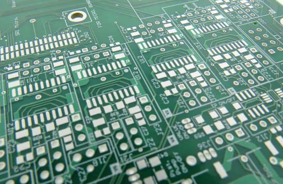
PCB surface treatment process gold plating, gold immersion and nickel palladium gold difference in which?
In the PCB surface treatment process, there are several treatment processes we often confuse: gold plating, gold immersion and nickel palladium gold; the difference between them is in?
1. Gold plating
Gold plating uses real gold, even if only a very thin layer of plating; it has accounted for nearly 10% of the cost of the entire board. Gold plating uses gold as the plating layer; one is to facilitate welding, and the second is to prevent corrosion; even after years of memory, gold fingers are still shiny as ever.
Advantages: strong electrical conductivity, good oxidation resistance, long life, dense plating, more wear-resistant, generally used in welding and plugging occasions.
Disadvantages: higher cost, poor welding strength.
2. Electroless gold/immersed gold
Electroless nickel dip gold (ENIG), also known as electroless nickel gold, sink nickel gold, referred to as electroless gold and pink gold. Immersion gold is through chemical methods; the copper surface is wrapped in thick, good electrical properties of the nickel-gold alloy and can protect the PCB for a long time. The inner layer of nickel deposition thickness is generally 120 ~ 240μin (about 3 ~ 6μm), and the outer layer of gold deposition thickness is generally 2 ~ 4μinch (0.05 ~ 0.1μm). Immersion gold can make the PCB use the process in the long term to achieve good electrical conductivity. However, other surface treatment processes do not have tolerance for the environment.
Advantages: 1. Immersion gold treated PCB surface is very flat, coplanarity is very good, suitable for key contact surface. 2. Immersion gold has excellent solderability; gold will move quickly into the melting solder inside, forming metal compounds.
Disadvantages: the process is complex, and to achieve good results needs to control the process parameters strictly. The most troublesome is that the surface of the PCB treated with sunken gold is easy to produce black disc benefits, affecting reliability.
3. Chemical nickel palladium gold
Compared with the chemical nickel gold, chemical nickel palladium gold (ENEPIG) in the nickel and gold between the extra layer of palladium, in the deposition reaction of replacement gold, the chemical palladium layer will protect the nickel layer to prevent it from being cross replacement gold excessive corrosion; palladium in the prevention of corrosion caused by the replacement reaction at the same time, for the immersion of gold to prepare fully. The deposition thickness of a nickel is generally 120~240μin (about 3~6μm); the thickness of palladium is 4~20μin (about 0.1~0.5μm); the deposition thickness of gold is generally 1~4μin (0.02~0.1μm).
Advantages: wide range of applications, while the nickel palladium gold chemistry, relative to gold deposition, can effectively prevent the black disk defects caused by connection reliability problems.
Disadvantages: Although nickel palladium chemistry has many advantages, palladium is expensive and is a shortage of resources. Also, like sunken gold, its process control requirements are strict.
Summary
This article has introduced some PCB surface treatment processes and how they differ. PCB surface treatment processing is an essential process in the PCB production process. It is to protect the surface of the PCB circuit board. Suppose a PCB needs to be designed and manufactured. In that case, Anpllopcb will be there from the beginning of the project to the finish line, and we will be in constant contact with you to keep you informed of the entire process, from manufacturing to assembly. This can help you save money and stress with lower PCB costs, shorter wait times and higher-quality products. We want to save you time and effort so you can focus on your PCB design – without worrying about the nitty-gritty of the manufacturing process.

