- How to distinguish PCB through-hole, blind Hole, buried hole hole
- What is the difference between blind holes and buried holes?
- What are the benefits of blind and buried holes?
- So how do you build blind and buried holes?
- Choose the right PCB manufacturer for blind and buried holes.
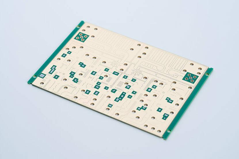
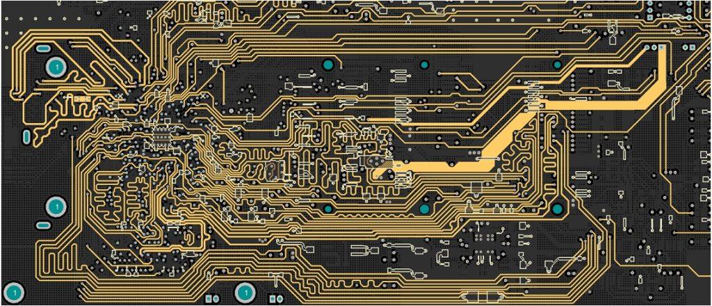
In PCB manufacturing, over-hole design is an important factor; it consists of holes, pads around the hole area and POWER layer isolation area, usually divided into blind, buried hole PCB, buried hole PCB and through-hole PCB three categories. So also often encountered about what is blind and buried holes respectively? The advantages of blind and buried holes and their construction, as well as how to properly add blind and buried holes on the printed circuit board. In the ordinary case, installing all the links needed on the PCB on one layer is not easy. The solution to this problem is through-hole. They are shaped like barrel-shaped conductive holes and can be connected in multiple layers between circuit boards.
At present, the design and manufacture of high-speed PCBs are widely used in communications, computers, graphics image processing, and other fields, all high-tech value-added electronic product design in the pursuit of low power consumption, low electromagnetic radiation, high reliability, miniaturization, lightness and other characteristics, in order to achieve the above goals, in the high-speed PCB design and manufacture, the design of through-hole is an important factor.
How to distinguish PCB through-hole, blind Hole, buried hole hole
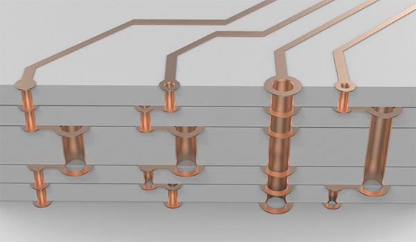
In general, we often see PCB design guide holes in three ways, respectively.
① Through Hole
Through-hole: Placing a Through Hole, abbreviated as PTH, is the most common one; you hold the PCB up to the light, and you can see the bright hellhole is the “through-hole. This is also the simplest kind of hellhole because the production, as long as the use of a drill or laser directly to the board to do all the drilling can be, the cost is relatively cheap. However, some circuit layers do not need to connect these holes. Therefore, although the through-hole is cheap, sometimes it will use up more PCB space.
② Blind Via Hole
Blind Via Hole: Blind Via Hole, the outermost circuit of the PCB is connected to the adjacent inner layer with plated holes because the opposite side is not visible, so it is called “blind via”. In order to increase the space utilization of the PCB circuit layer, the “Blind Via Hole” process was created. This production method requires special attention to the depth of drilling (Z-axis) to be just right, but this method often causes plating difficulties in the Hole, so almost no manufacturers use it; it can also be connected in advance to the circuit layer in the individual circuit layer when the hellhole is first drilled, and then glued together, but requires more sophisticated positioning and alignment devices.
③ Buried Hole
Buried Hole: The connection of any circuit layer inside the PCB but not connected to the outer layer. Drilling holes cannot achieve this process after bonding. However, it must be performed at the time of individual circuit layers, first partially bonding the inner layers and then plating before finally bonding them all, which is more laborious than the original “through holes” and “blind holes” and, therefore, the most expensive. This process is usually only used in high-density (HDI) circuit boards to increase the available space for other circuit layers.
What is the difference between blind holes and buried holes?
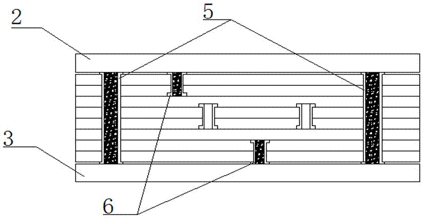
Although there is more than one type of through-hole, the two most commonly used are. Both are blind and buried through-hole. A blind hole connects the outer layer of the board to one of the inner layers. However, it cannot always be present throughout the PCB. The through-hole can connect the inner layer without reaching the outer layer. In addition, a through-hole is set up, which passes vertically through the entire board and connects all layers. This concept is relatively simple to understand and can offer some advantages.
What are the benefits of blind and buried holes?
Some PCB designs are relatively small, and it has limited space. Therefore, blind and buried holes can provide more space and options for the plate. For example, buried vias will help free up space on the board without affecting the surface devices or alignments on the top and bottom layers. Blind vias help free up more space. They are often used for pitch BGA assemblies. Because blind holes only go through part of the thin board, this also means that less signal residue can be left behind.
Although blind and buried vias can be used on many PCB designs, they are typically used for high-density interconnect PCBs or HDI. HDI can provide better power transfer and higher layer density. Hidden vias, which also help make the board smaller and lighter, are useful for making electronics. They are often used in medical devices, computers, cell phones, and small electronics worn.
While blind holes and buried pits can help those who need them, they can also increase the cost of producing PCBs. This is because of the extra work required to add to the board and the required testing and fabrication. This means that they are only used when needed; you want a board that is both compact and efficient.
So how do you build blind and buried holes?
Through-holes can be formed before or after multiple layers are pressed. Blind and buried via holes added to the PCB by drilling are unstable. It is important that the builder knows and understands the depth of the drill bit. If the Hole is not deep enough, there is not a good connection. If the cavity is too deep, the signal quality will be degraded, or distortion will result. If these things happen, it is not possible.
For blind holes, different drilling information is needed to determine the holeHole. The hole diameter ratio to the drill diameter should be equal to or less than. The smaller the cavity, the smaller the distance between the outer and inner layers.
When burying holes, different drill files are needed to create each holeHole. This is because they are connected to different parts of the inner layer of the plate. The ratio between the Hole’s depth and the drill bit’s diameter should not exceed 12. If it is larger than this diameter, it may touch other connecting plates.
Choose the right PCB manufacturer for blind and buried holes.
Designing blind and buried vias in PCBs is a delicate process best determined by a specialized manufacturer. This means that finding the right manufacturer becomes very important. Anpllopcb offers various services and technologies that can help simplify your life. Depending on your needs, we can provide a simple design or a complex board. There are many benefits to working with us. We offer 24/7 support and fast lead times. We also offer instant online quotes for SMT placement to give you an idea of how much your project will cost and how to track your order. Please contact us if you have any questions about blind and buried vias.

