- 1, ultra-thick copper multilayer PCB manufacturing process
- 2, ultra-thick copper PCB finished effect
- 3、Summary
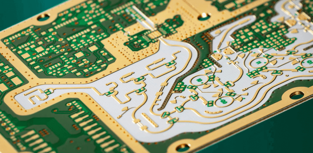
Special ultra-thick copper multilayer PCBs originated in North America, such as the Canadian company UPE. The company began to develop and produce ultra-thick copper multilayer PCBs in the 1990s and achieved good results. This type of special board product is used in strong current connection transmission as well as strong and weak mixed connection components, according to market information, in automotive electronics, IGBT assembly, wind power converters, ignition coils, etc., are in demand; on the other hand, with the widespread use of printed circuit boards in the electronics field, the functional requirements are increasingly high, printed circuit boards will not only provide the necessary electrical connection for electronic components As well as mechanical support, but also gradually given more additional functions, and thus can be integrated into the power supply, providing high current, high reliability of the ultra-thick copper multilayer PCB gradually become a new product developed by the PCB industry, broad prospects, profit margins than traditional circuit boards to be larger, with a very large development value. Ultra-thick copper multilayer PCBs will occupy an important position in the future high-end circuit connection market and will inevitably usher in broader market prospects.
Currently, the industry is generally used to electroplated copper plating thickened one by one, and multiple solders resist the printing-assisted accumulation of layers or the use of ultra-thick copper foil to achieve ultra-thick copper printed circuit board manufacturing. Nevertheless, the above-process copper thickness can only reach a maximum of 0.41 mm (12 oz/ft²), more than this copper thickness, processing ultra-thick copper multilayer board will become very difficult, and there is no technical breakthrough in this area. The difference between ordinary PCBs and ultra-thick copper PCBs are shown in Table 1. This paper focuses on a new process method for manufacturing ultra-thick copper multilayer PCBs, more than 0.5 mm (14 oz/ft²) of ultra-thick copper multilayer printed circuit board manufacturing.
1, ultra-thick copper multilayer PCB manufacturing process
1.1 Stacked layer structure
This paper focuses on a super-thick copper three-layer board with an inner copper thickness of 1.0 mm, an outer copper thickness of 0.3 mm, an outer minimum line width line spacing of 0.5 mm, and a laminated structure. The surface layer is FR4 copper-clad board (glass fiber epoxy resin copper-clad board) with a thickness of 0.3 mm and single-sided etching treatment, and the bonding layer is a non-fluid PP sheet (semi-curing sheet) with a thickness of 0.1 mm. The super-thick copper board is embedded in the corresponding hole structure with FR-4 epoxy board.
The processing process of super-thick copper PCB is mainly machined with the surface and mid-layer milling board, thick copper board number milling, after surface treatment, stacked in the overall mold temperature pressed together, after demolding according to the PCB conventional process to complete the finished product production.
1.3 Key process methods
1.3.1 Super-thick copper lamination technology
Super-thick copper inner lamination: super-thick copper if the use of copper foil will be difficult to achieve this thickness, this paper super-thick copper inner layer using a 1 mm electrolytic copper plate; the conventional material is easy to purchase; the milling machine directly processing molding; the inner layer of copper plate outer contour using the same thickness of FR4 plate (glass fiber epoxy resin plate) processing molding as a whole filling, in order to facilitate the stacking and to ensure that it fits closely with the copper plate periphery, the gap between the two contours is controlled to be within 0~0.2 mm. With the filling effect of FR4 board, the copper thickness problem of the super-thick copper board is solved, and it ensures the tight pressing and internal insulation problem after lamination so that the design of inner copper thickness can be more than 0.5 mm.
1.3.2 Ultra-thick copper blackening technology
The blackening of the copper plate can increase the surface area of the copper surface in contact with the resin and increase the wetting of the copper by high-temperature flowing resin so that the resin can penetrate deep into the oxidation layer voids and show strong adhesion after hardening, which improves the lamination effect. At the same time, it improves the laminate white spot phenomenon and baking test (287 ℃ ± 6 ℃) caused by the plate surface whitening, bubbles, and other problems.
1.3.3 Super-thick copper PCB lamination technology
Due to the manufacturing error of the inner layer of the super-thick copper board and the thickness of the FR-4 board for peripheral filling, the thickness cannot be the same; if the conventional laminating method is used, it is easy to produce laminating white spots, delamination, and other defects, and it is not easy to laminate. In order to reduce the difficulty of lamination and ensure the dimensional accuracy of the super-thick copper layer, the lamination effect is achieved by setting the appropriate lamination temperature, pressure, holding time, and other process parameters and solving the technical problems of lamination white spots and delamination of super-thick copper to meet the lamination requirements of super-thick copper PCB. The process parameters can achieve the lamination effect and solve technical problems such as white spots and delamination of ultra-thick copper lamination to meet the lamination requirements of ultra-thick copper PCB.
(1) Ultra-thick copper PCB lamination method.
Super-thick copper lamination mold in the stacking level of the product. Due to the low mobility of non-fluid PP resin, if the use of conventional laminated material kraft paper, the PP sheet can not be uniformly pressed, resulting in white spots, delamination, and other defects after lamination, thick copper PCB products in the lamination process requires the use of silicone mats as a key buffer layer, which plays a role in the uniform distribution of pressure in the lamination. In addition, to solve the lamination problem, the pressure parameter in the laminator is adjusted from 2.1 Mpa (22 kg/cm²) to 2.94 Mpa (30 kg/cm²), and the temperature is adjusted to the optimum fusion temperature of 170°C according to the characteristics of the PP sheet.
(2) Super-thick copper PCB lamination effect.
According to GJB362B-2009 chapter 4.8.5.8.2, after the test, according to 4.8.2, an inspection of PCB should be no more than 3.5.1.2.3 chapter (subsurface defects) allowed blistering and delamination. PCB specimens meet the requirements of 3.5.1 appearance and size and its microscopic cut, and according to 4.8.3 inspection, in line with the requirements of 3.5.2. From the condition of the laminated slices, the lines are filled to the brim with no micro steam bubbles.
1.3.4 Ultra-thick copper PCB flow control technology
Unlike the general PCB processing, the shape and device connection holes in the lamination have been completed before; if the flow of glue will seriously affects the roundness and size of the connection, the appearance and use can not meet the requirements; this process development has also been tested first pressed together after milling the shape of the process route, but the shape of the later milling requirements for strict control, especially the processing of the inner layer of thick copper connection parts, its depth accuracy control is very strict, the pass rate is extremely low The rate of passing is extremely low.
Selecting the appropriate bonding material and designing a reasonable device structure is one of the difficulties in the research. In order to solve the problem of overflowing adhesive appearance caused by ordinary semi-cured sheets after lamination, a low-fluidity semi-cured sheet (SangYi: SP120N) is used, which is a bonding material with low resin flow, flexibility, excellent heat resistance, and electrical properties. According to the characteristics of overflowing adhesive, the semi-cured sheet profile at a specific location is released. A specific shape profile is processed by using the cut-and-draw method. At the same time, the process of forming first and then pressing together is performed. The shape is formed after pressing together, without needing CNC milling shape processing so that the PCB in the lamination after the flow of glue phenomenon has been solved to ensure that the ultra-thick copper board lamination after the connection surface has no glue flow and is pressed tight.
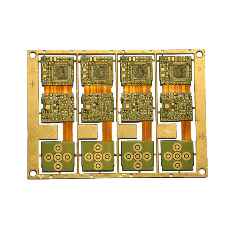
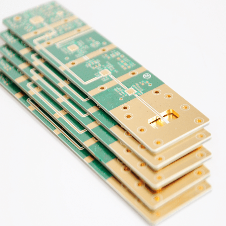
2, ultra-thick copper PCB finished effect
2.2.1 Pressure test
The super-thick copper PCB samples of each pole for voltage testing, a test voltage of AC1000V, 1 min no hit, flash phenomenon.
2.2.2 High current temperature rise test
Design the corresponding copper plate to the ultra-thick copper PCB samples in the series connection of the poles and access to the high current generator, according to the corresponding test current. Super-thick copper PCB overall temperature rise is relatively low to meet the actual use of the requirements (general temperature rise requirements in the 30 K or less). Super-thick copper PCB’s high current temperature rise is related to its structure; the temperature rise of different thick copper structures will have some differences.
2.2.3 Thermal stress test
Thermal stress test requirements: according to GJB362B-2009 rigid printed circuit board general specifications for the sample after the thermal stress test, visual inspection, no delamination, blistering, pad warping, white spots, and other defects.
PCB specimen appearance and size must be microdissection. Because the inner layer of this sample is too thick copper, it can not be a metallographic section, so the sample at 287 ℃ ± 6 ℃ after the thermal stress test, only the visual inspection of its appearance.
The test results show no delamination, blistering, pad warping, white spots, and other defects.
3、Summary
This paper provides a super-thick copper multilayer PCB manufacturing process method, through technological innovation and process improvement, effectively solving the current super-thick copper multilayer PCB copper thickness limitations, breaking the standard processing technology problems as follows.
(1) super-thick copper inner layer lamination technology: solves the problem of super-thick copper material selection, using a pre-milling molding process without etching, effectively avoiding the thick copper board etching technical problems; through FR-4 filling technology to ensure that the inner layer is pressed together tightly and insulation problems.
(2) Ultra-thick copper PCB lamination technology: effectively solve the problem of lamination white spots and delamination, and find a new way of pressing and solution.
(3) Ultra-thick copper PCB flow control technology: effectively solves the problem of flowing glue after lamination and ensures the implementation of the process of pre-milling shape and then lamination.

