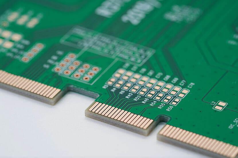
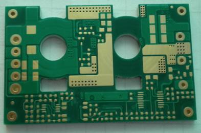
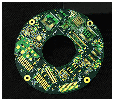
Via, also known as metallization holes, is one of the important components of PCB design. In double-sided and multilayer boards, to connect the printed wires between the layers, a common hole is drilled at the wires that need to be connected in each layer, that is, vias. There are three types of vias, namely blind via, buried via and through via.
Pcb via hole design top ten questions answered.
01
Often, the PCB board has a lot of holes; the more holes, the better. Are there any rules?
A: No. To minimize the use of vias, when you have to use vias, you should also consider reducing the impact of vias on the circuit.
02
When laying out the board, if the lines are dense, the vias may have to be more, which will affect the board’s electrical performance; how can I improve the board?
A: For low-frequency signals, it doesn’t matter if there are too many holes; high-frequency signals try to reduce the number of holes. If there are more lines, you can consider multilayer boards.
03
How big is the effect of through-hole and blind-hole on the signal difference? What is the principle of application?
A: Using blind or buried holes is an effective way to increase the density of multilayer boards, reduce the number of layers and board size, and greatly reduce the number of plated through holes. However, a through-hole is good to achieve in process and lower cost, so generally, a through-hole is used in the design.
04
Can you explain the proportional relationship between the line width and the size of the matching through-hole?
A: It is difficult to say there is a simple proportional relationship because the two simulations are different. One is a surface transmission, and the other is a ring transmission. You can find impedance calculation software on the Internet and keep the impedance of the vias and transmission line impedance consistent.
05
What is the relationship between the width of the line on the PCB and the size of the vias, and the size of the current passed?
A: The general PCB copper foil thickness of 1 ounce, about 1.4 miles, and roughly 1 mil line width allow the maximum current of 1A. Via hole is more complex, in addition to the size of the via pad, but also with the processing of plating after the thickness of the hole wall sink copper.
06
Do you need to match the Sqrt(L/C) of the vias according to the requirements?
A: Yes, simply put, impedance matching, adjusting the parameters of the vias to achieve a better impedance smooth transition.
07
Is there a corresponding relationship between temperature change and the impedance of the vias?
A: The temperature change mainly affects the reliability of the vias, and the material selection is required to consider the CTE value of the material.
08
What is a good suggestion for a high-speed PCB, a wiring process, and how to avoid vias?
A: For High-speed PCBs, it is best to play less through-hole by increasing the signal layer to solve the need to increase the need for through-hole.
09
What is the role and principle of adding grounding vias near the alignment?
A: PCB board vias, classified by their role, can be divided into the following categories.
(1) signal vias (vias structure requires minimal impact on the signal)
(2) power supply, ground vias (vias structure requires the minimum distribution of inductance vias)
(3) heat dissipation through-hole (through-hole structure requires the minimum thermal resistance of the through-hole)
The vias mentioned above belong to the grounding type vias, and the role of the grounding vias near the alignment vias is to provide the shortest return path for the signal.
Note: the signal for the layer of the perforation is an impedance discontinuity; the signal return path will be disconnected from here; to reduce the signal return path surrounded by the area, the signal perforation must be played around some ground perforation to provide the shortest signal return path, reduce the signal EMI radiation. This radiation will increase significantly with the increase in signal frequency.
10
Signal vias aperture diameter is relatively small (such as 0.3mm diameter); in this case, will not be enough vias metallization?
A: If the hole diameter is small and deep (i.e., the hole diameter is relatively large), there is a possibility that it will not be fully metallized.
Choose the right PCB manufacturer.
Designing vias on PCBs is best decided by a professional manufacturer. This means that finding the right PCB manufacturer becomes very important. Anpllopcb can provide various services and technologies to help you streamline your supply chain process. We can provide simple designs or complex boards depending on your needs.
There are many benefits to working with us. We provide 24/7 support and offer fast lead times. We also offer instant online quotes for SMT placement to give you an idea of how much your project will cost and how to track your order. Please get in touch with us if you have any questions about blind and buried vias.

