- General PCB design checklist items
- PCB electrical characteristics check items
- PCB physical characteristics check items
- PCB mechanical design factors
- PCB printed circuit board mounting requirements
- Printed circuit board dial-out requirements
- PCB mechanical considerations
- PCB Electrical Considerations
- PCB wiring path and positioning
- PCB width and thickness
- PCB wire spacing
- PCB wire graphics check
- PCB design project checklist of items
- Conclusion
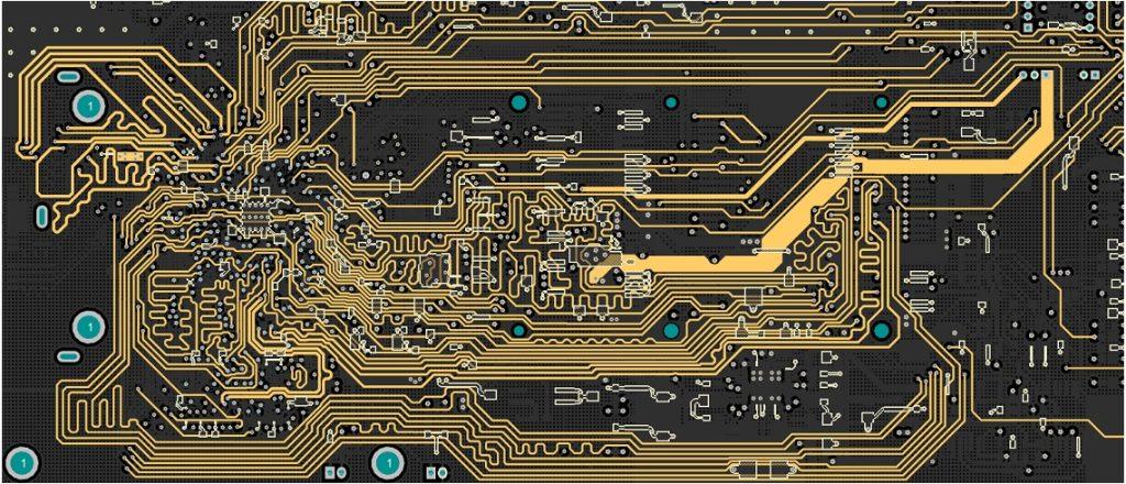
In the design, the layout is an important part. The result of the layout will directly affect the effect of wiring, so it can be considered that a reasonable layout is the first step in the success of PCB design. Especially pre-layout is the process of thinking about the whole board, signal flow, heat dissipation, structure and other architecture. If the pre-layout fails, the later effort is also in vain.
PCB layout design printed wiring board design process includes the design of schematics, electronic components database login, design preparation, block division, electronic components configuration, configuration confirmation, wiring and final inspection. During the process flow, no matter in which process a problem is found, it must be returned to the previous process for re-confirmation or correction. The following checklist includes all aspects of the design cycle, for special applications should also add some additional items.
General PCB design checklist items
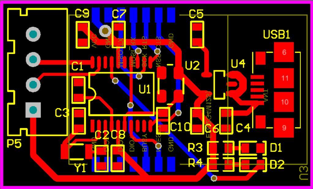
(1) circuit analysis has not? To smooth the signal circuit is divided into basic units.
(2) does the circuit allows the use of short or isolated key leads?
(3) must be shielded in place, effectively shielded?
(4) Is the basic grid pattern fully utilized?
(5) Is the size of the printed circuit board the best size?
6) Are the selected lead widths and spacing used as much as possible?
(7) whether the use of the preferred pad size and hole size?
(8) Is the photographic base and sketch appropriate?
9) Is the minimum jumper wire used? Do the jumper wires go through the components and accessories?
(l0) Are the letters visible after assembly? Are the dimensions and type correct?
(11) Is there a window in the large copper foil area to prevent blistering?
12) Is there a tool positioning hole?
PCB electrical characteristics check items
1) Has the impact of wire resistance, inductance, and capacitance been analyzed? In particular, the critical voltage drop phase ground shadow analysis?
(2) Is the spacing and shape of the wire attachment in line with the insulation requirements?
(3) Is the insulation resistance value controlled and specified in the critical place?
(4) Is the polarity adequately identified?
(5) from the geometric point of view, to measure the spacing of the wire on the leakage resistance, voltage impact?
6) Is the medium for changing the surface coating layer identified?
PCB physical characteristics check items
(1) Are all pads and their locations suitable for general assembly?
(2) Can the assembled printed circuit board meet the impact and vibration conditions?
3) What is the spacing of the specified standard components?
(4) Is the installation of unsecured components or heavier parts fixed?
5) Is the cooling of heat-generating components correct? Or with the printed circuit board and other thermal components isolated?
(6) voltage dividers and other multi-lead components are correctly positioned?
(7) component arrangement and orientation to facilitate inspection?
(8) Are all possible interferences on the printed circuit board and the entire printed circuit board assembly eliminated?
9) Are the dimensions of the positioning holes correct?
10) Are the tolerances complete and reasonable?
11) Have the physical characteristics of all coating layers been controlled and signed?
12) Is the hole-to-lead diameter ratio within acceptable limits?
PCB mechanical design factors
Although the printed circuit board takes mechanical methods to support the components, it cannot be used as a structural part of the entire device, in the edge part of the printed circuit board, at least every 5 inches for a certain amount of text support.
The following factors must be considered in the selection and design of the printed circuit board.
1) The structure of the printed circuit board – size and shape.
2) The type of mechanical accessories and plugs (holders) required.
3) The adaptability of the circuit to other circuits and environmental conditions.
4) Depending on several factors, such as exposure to heat and dust, consider vertical or horizontal mounting of the printed circuit board.
(5) need to pay special attention to environmental factors, such as heat dissipation, ventilation, shock, vibration, and humidity. Dust, salt spray, and radiation lines.
6) The degree of support.
7) Hold and fix.
8) Easy to take down.
PCB printed circuit board mounting requirements
At least should be supported within 1 inch of the edge of the three edges of the printed circuit board. According to practical experience, the thickness of 0.031 – 0.062 inches of printed circuit board support point spacing should be at least 4 inches; the thickness greater than 0.093 inches of the printed circuit board, the support point spacing should be at least 5 inches. This measure can be taken to improve the rigidity of the printed circuit board and destroy the possible resonance of the printed circuit board.
Some printed circuit boards usually have to consider the following factors before deciding on their mounting techniques.
1) The size and shape of the printed circuit board.
2) The number of input and output terminals connected.
(3) The available equipment space.
4) The desired ease of loading and unloading.
5) mounting accessories.
6) Required heat dissipation.
7) The required shielding.
8) The type of circuitry and the interrelationship with other circuits.
Printed circuit board dial-out requirements
1) The printed circuit board area does not require the installation of components.
2) The influence of the plugging tool on the installation distance between the two printed circuit boards.
3) In the design of the printed circuit board to be specially prepared for the installation of holes and slots.
(4) plug and dial tool to be placed in the device when used, especially considering its size.
5) A plugging device is required, which is usually permanently fixed to the printed circuit board assembly with rivets.
(6) The printed circuit board’s mounting rack requires special designs, such as a load-bearing flange.
(7) the plugging tool used and the size, shape and thickness of the printed circuit board adaptability.
(8) the use of plugging tools involves the cost, including both the price of tools and the increased expenditure.
(9) To fasten and use the plugging tool and the requirement for a certain degree of access to the device’s interior.
PCB mechanical considerations
Printed circuit assemblies impact the substrate characteristics: water absorption, thermal expansion coefficient, heat resistance characteristics, flexural strength, impact strength, tensile strength, shear strength and hardness. All of these properties affect both the functionality and productivity of the printed circuit board structure.
For most applications, the dielectric substrate for printed circuit boards is one of the following substrates.
1) Phenolic-impregnated paper.
(2) acrylic-polyester-impregnated irregularly arranged glass mat.
(3) Epoxy-impregnated paper.
(4) Epoxy-impregnated glass cloth.
Each substrate can be flame retardant or combustible. 1, 2 and 3 above are punchable. The most commonly used material for metalized hole-printed circuit boards is epoxy-glass cloth, which is dimensionally stable for high-density circuit use and minimizes the occurrence of cracks in the metalized holes.
One disadvantage of epoxy-glass cloth laminates is that they are difficult to punch in the common thickness range of printed circuit boards. For this reason, all holes are usually drilled out, and a profiling milling operation is used to form the shape of the printed circuit board.
PCB Electrical Considerations
In DC or low-frequency AC applications, the most important electrical characteristics of the insulating substrate are insulation resistance, resistance to electrical isolation and printed wire resistance, and breakdown strength.
In high frequency and microwave applications, they are dielectric constant, capacitance, and dissipation factor.
And in all applications, the current loading capability of the printed wire is important.

PCB wiring path and positioning
Printed wires should take the shortest route between components within the constraints of the specified wiring rules. Coupling between parallel wires should be limited as much as possible. A good design requires a minimum number of wiring layers and, corresponding to the required package density, requires using the widest wires and the largest pad size. Because rounded corners and smooth internal bed corners may avoid some electrical and mechanical problems, sharp corners in the wires should be avoided.
PCB width and thickness
The load capacity of copper conductors etched on rigid printed circuit boards. For 1 ounce and 2 ounces of wire, taking into account the normal variation in etching methods and copper foil thickness, as well as temperature differences, allow a reduction of 10% of the nominal value (in terms of load current); for printed circuit board assemblies coated with a protective layer (substrate thickness of fewer than 0.032 inches, copper foil thickness of more than 3 ounces) then components are reduced by 15%; for dip-soldered printed circuit boards are allowed to reduce by 30%.
PCB wire spacing
The minimum spacing of wires must be determined to eliminate voltage breakdown or flying arcs between adjacent wires. The spacing is variable, and it depends mainly on the following factors.
1) The peak voltage between adjacent wires.
(2) atmospheric pressure (maximum working height).
3) The coating layer used.
4) Capacitive coupling parameters.
Critical impedance or high-frequency elements are placed close together to minimize critical stage delays. Transformers and inductive components should be isolated to prevent coupling; inductive signal leads should be laid out orthogonally at right angles; components that generate any electrical noise due to magnetic motion should be isolated or rigidly mounted to prevent excessive vibration.
PCB wire graphics check
(1) Are the wires short and straight without sacrificing functionality?
2) Are the limits of the wire widths observed?
(3) between the wires, between the wires and mounting holes, between the wires and pads….. must ensure that the minimum wire spacing is left out?
(4) whether to avoid all the wires (including component leads) closer to a similar layout.
5) Are sharp angles (90°C or less) avoided in the wiring pattern?
PCB design project checklist of items
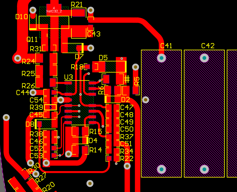
1. check the reasonableness and correctness of the schematic diagram.
2. check the correctness of the component package of the schematic diagram.
3. the spacing of strong and weak power and isolation areas.
4. check the correspondence between the schematic and the PCB diagram to prevent the loss of the network table.
5. whether the package of components and the physical match.
6. Whether the placement of components is appropriate.
A. Whether the components are easy to install and remove.
B. Whether the temperature-sensitive components are too close to the heat-generating components.
C. can produce mutual inductance components if distance and direction are appropriate.
D. Whether the placement between the connectors corresponds smoothly;
E. ease of unplugging.
F. input and output.
G. strong and weak power.
H. Whether the digital and analogue are interleaved.
I. an arrangement of upwind side and downwind side components.
7. whether components with directional characteristics are incorrectly flipped instead of rotated.
8. whether the mounting holes of the component pins are suitable and can be inserted easily.
9. check whether the empty leg of each component is normal and whether it is a leaky line.
10. check whether the same network table has holes in the upper and lower layers of wiring and whether pads are connected through the holes to prevent disconnection and ensure the line’s integrity.
11. check whether the upper and lower layers of character placement are correct and reasonable. Do not put on the components to cover the character to facilitate the operation of welding or maintenance personnel.
12. very important connection of the upper and lower lines; do not just use the pads of the components connected by direct insertion. It is best also to use the over-hole connection.
13. the arrangement of power and signal lines in the socket ensures the signal’s integrity and anti-interference.
14. pay attention to the appropriate ratio of pads and solder holes.
15. each plug is as far as possible on the edge of the PCB and easy to operate.
16. check whether the component markings are consistent with the components. The components are placed as far as possible in the same direction and placed neatly.
17. To avoid violating the design rules, power and ground should be as thick as possible.
18. Generally, the upper layer goes horizontal lines, the lower layer goes vertical lines, and chamfering is not less than 90 degrees.
19. the size and distribution of the mounting holes on the PCB are appropriate to reduce the PCB bending stress as much as possible.
20. pay attention to the height distribution of components on the PCB and the shape and size of the PCB to ensure easy assembly.
Conclusion
For engineers, it is important to have enough expertise in PCB design to judge the quality of one staff design. However, engineers without expertise can view the above methods. It is always a good idea to always have an expert check the quality of a PCB design before transitioning to pcb prototyping, especially when designing starter products.


