- PCB design for manufacturability, design for assembly
- The 8 principles of PCBA manufacturability design
- 1. Preferred surface assembly and crimp components
- 2. To PCBA assembly surface as the object, the overall consideration of the package scale and pin spacing
- 3. Shorten the process path
- 4. Optimize the layout of components
- 5. Overall consideration of the design of the pad, solder resist and stencil window
- 6. Focus on the new package
- 7. Focus on BGA, chip capacitors and crystal oscillators
- 8. Research cases to improve the design rules
- What issues should be noted in the design of PCBA board manufacturability?
- Summary
PCB design for manufacturability, design for assembly
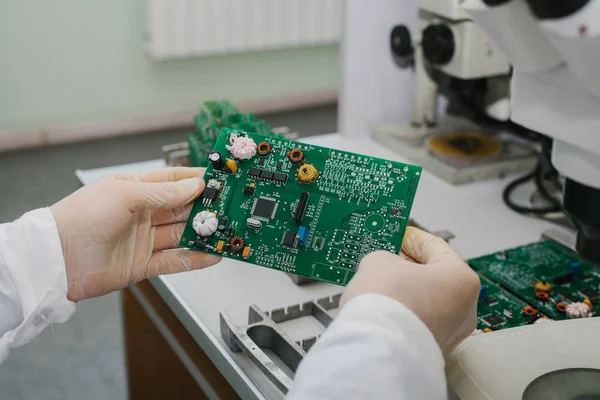
Many people have been wondering, where is the difference between PCBA and PCB? PCBA manufacturability design includes PCB manufacturability design and PCBA assembly design (or assembly design).
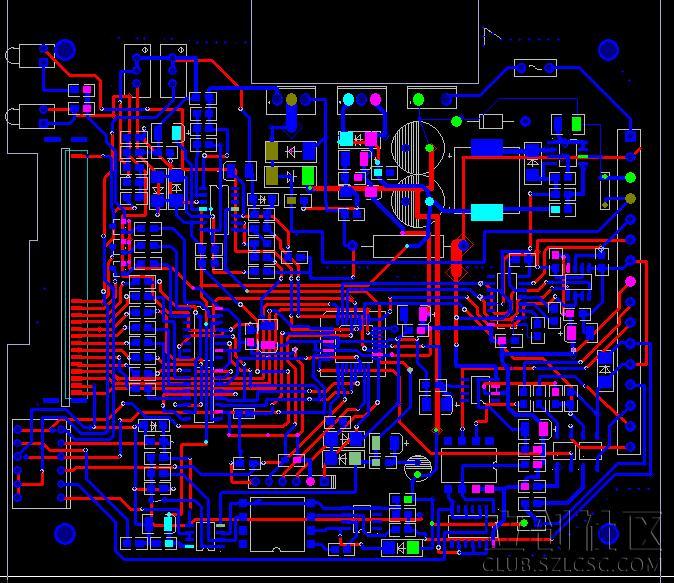
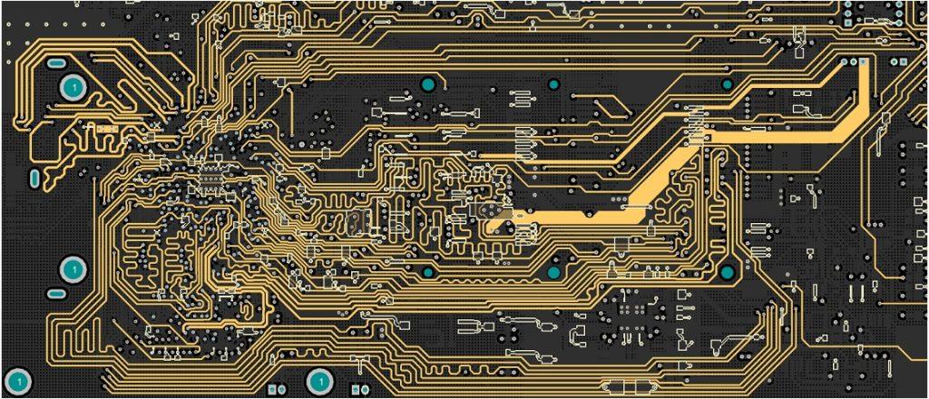
PCB manufacturability design to “manufacturability” as the focus of the design content, including board selection, crimping structure, hole ring design, resistance welding design, surface treatment and assembly design. These designs are related to the processing capability of the PCB. Restricted by processing methods and capabilities, the design of the minimum line width and line spacing, minimum hole diameter, minimum solder ring width and minimum resistance gap must meet the processing capabilities of the PCB, the design of the laminate crimp structure must meet the PCB processing process. Therefore, the PCB manufacturability design’s focus is to meet the PCB factory’s process capability. Understanding the PCB manufacturing method, process flow, and capability is the basis for implementing the process design.
The focus of PCBA manufacturability design is “assembly”, that is, to establish stable and solid manufacturability, to achieve high quality, high efficiency, and low cost of soldering. The design includes packaging selection, liner design, assembly method design, part layout, wire mesh design, Etc. These design requirements focus on higher weld yield, higher manufacturing efficiency, and lower manufacturing costs. Therefore, it is important to understand the process characteristics of various packages, common bad soldering phenomena and the factors affecting them.
Whether the PCB manufacturability design or PCBA manufacturability design can not simply focus on individual design elements, in the design, the manufacturability of the single board must be considered comprehensively and systematically, that is, repeat the strength of the “integrated” design concept.

The 8 principles of PCBA manufacturability design
1. Preferred surface assembly and crimp components
Surface assembly components and crimp components, with good processability.
With the development of component packaging technology, most components can be bought in a package category suitable for reflow soldering, including cartridge components that can be reflow soldered using a through-hole. If the design can achieve full surface assembly, it will greatly improve the efficiency and quality of the assembly.
Crimp components are mainly multi-pin connectors; this type of package also has good processability and reliability and is also the preferred category.
2. To PCBA assembly surface as the object, the overall consideration of the package scale and pin spacing
The package scale and pin spacing are the biggest impacts on the whole board process. The premise of selecting the surface assembly components must be for a specific size and assembly density of the PCB, select a group of packages similar to the process, or that is suitable for a certain thickness of stencil for solder paste printing package. For example, the selected packages of cell phone boards are suitable for solder paste printing with 0.1mm thick stencil.
3. Shorten the process path
The shorter the process path, the higher the productivity and the more reliable the quality. The preferred process path design is:
(1) single-sided reflow soldering.
(2) Double-sided reflow soldering.
(3) double-sided reflow soldering + wave soldering.
(4) Double-sided reflow soldering + selective wave soldering.
(5) double-sided reflow soldering + hand soldering.
4. Optimize the layout of components
The principle component layout design mainly refers to the layout of components and spacing design. The layout of the components must meet the requirements of the welding process. A scientific and reasonable layout can reduce the use of bad solder joints and tooling and optimize the stencil’s design.
5. Overall consideration of the design of the pad, solder resist and stencil window
The solder pad design, solder resist and stencil window determine the amount of solder paste distribution and the process of forming solder joints. Coordinating the design of pads, solder resist, and stencil has a very big role in improving the solder throughput.
6. Focus on the new package
The so-called new packages do not exactly refer to the new packages on the market but to those that your company has no experience using. For the introduction of new packages, small batch process verification should be conducted. Just because someone else can use it does not mean you can use it too. The prerequisite for using it must be to have done the test, understand the process characteristics and problem spectrum, and master the countermeasures.
7. Focus on BGA, chip capacitors and crystal oscillators
BGA, chip capacitors and crystals are typical stress-sensitive components; the layout should be avoided as far as possible when placed on the PCB in the welding, assembly, shop turnover, transportation, use and other links prone to bending deformation.
8. Research cases to improve the design rules
According to the continuous emergence of poor assembly or failure cases, manufacturing design rules from the production practice continue to optimize and improve the design rules, to improve the design of manufacturability, which has a very important significance.

What issues should be noted in the design of PCBA board manufacturability?
1. Minimize the number of PCB layers. Can use a single panel without a double panel, can use a double panel without a multilayer board, and try to reduce PCB processing costs.
2, try to use the reflow soldering process because reflow soldering has more superiority than wave soldering.
3、 Minimize the PCB assembly process; try to use the no-cleaning process.
4, whether to meet the SMT process and equipment requirements for PCB design.
5、Whether the Pcb shape and size are correct, and whether the small size PCB is considered for the assembly process.
6、Is the clamping edge design and positioning hole design correct?
7、Is the positioning hole and non-grounding mounting hole marked non-metallic?
8、Is the Mark graphic and its position by the regulations, and whether 1~1.5mm de-soldering area is left around it?
9、Whether the requirements of environmental protection are considered.
10, whether the choice of substrate materials, components and packaging meet the requirements.
11, PCB pad structure (shape, size, spacing) is in line with DFM specifications.
12、Whether the lead width, shape, spacing and connection between the lead and the pad meet the requirements.
13, the overall layout of components and components between the minimum spacing are in line with the requirements; large devices around whether to consider the size of the rework, the polarity of components arranged in the same direction as possible.
14, cartridge components aperture, pad design is in line with DFM specifications; adjacent cartridge components between the distance is conducive to manual cartridge operation.
15, solder resist film and screen graphics are correct, and component polarity and IC foot is marked out.
Summary
At present, the miniaturization and reliability of electronic products have been developed at high speed; it is necessary to pay great attention to the design of manufacturability, strive to create a corporate culture of manufacturability design, and improve the process of manufacturability design in the new product introduction process. Only by establishing a strict and perfect electronic product manufacturability design introduction process can we ensure that the designed products meet the current situation of the unit and establish a rapid response platform for PCB design and manufacturing.
Anpllopcb providing some of the most innovative printed circuit board technologies and highest quality standards in the industry. You can count on us to meet your needs, from the simplest boards to the most complex designs for small quantity and large scale production.


