- 1, the definition of over-hole
- 2, the parasitic capacitance of the through-hole
- 3、Parasitic inductance of the vias
- 4、Non-through hole technology
- 5, the general PCB over-hole selection
- 6, high-speed PCB in the design of the vias
- Select a PCB manufacturer suitable for blind and buried holes
In high-speed PCB design, over-hole design is an important factor; it consists of holes, pads around the hole area and POWER layer isolation area, usually divided into blind, buried hole PCB, buried hole PCB and through-hole PCB three categories. In the PCB design process, analysing the through-holes parasitic capacitance and parasitic inductance summarizes the knowledge of high-speed PCB through-hole design.
The current high-speed PCB design is widely used in communications, computers, graphics image processing, and other fields, all high-tech value-added electronic product design in the pursuit of low power consumption, low electromagnetic radiation, high reliability, miniaturization, lightness and other features, in order to achieve the above goals, in high-speed PCB design, through-hole design is an important factor.
1, the definition of over-hole
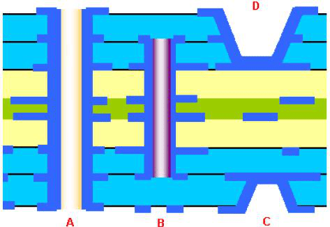
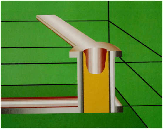
Over-hole is an important factor in the design of a multilayer PCB factory; an over-hole consists of three main parts, one is the hole; two is the pad area around the hole; three is the POWER layer isolation area. The over-hole process is the cylindrical surface of the hole wall in the hole with the chemical deposition method of plating a layer of metal. The middle layers need to connect the copper foil, and over the hole on the top and bottom of the two sides made of ordinary pad shape, can be directly connected to the top and bottom of the line, but also not connected. Perforation can play a role in electrical connection and fixed or positioning devices.
1) the hole is divided into blind, buried hole PCB, buried hole PCB and through-hole PCB
(1) blind holes
Blind holes refer to the top and bottom surface of the printed wiring board, with a certain depth; for the connection of the surface line and the following inner layer of the line, the depth of the hole and the hole diameter usually do not exceed a certain ratio.
(2) buried holes
Buried holes refer to the connection holes located in the inner layer of the printed circuit board; they do not extend to the surface of the circuit board.
Blind holes and buried holes are located in the inner layer of the circuit board; lamination before the through-hole moulding process to complete the process of forming the over-hole may also overlap several inner layers.
(3) Through-hole
Through-hole, this hole through the entire circuit board can be used to achieve internal interconnection or as a component mounting positioning holes. Because a through-hole in the process is easier to achieve, the cost is lower, so the general printed circuit board are used.

2, the parasitic capacitance of the through-hole
The through-hole itself has a parasitic capacitance to ground if the through-hole in the layered isolation hole diameter is D2, the diameter of the through-hole pad is D1, the thickness of the PCB is T, the board substrate dielectric constant is ε, the size of the parasitic capacitance of the through-hole is approximated by
C =1.41εTD1/(D2-D1)
The main impact of the parasitic capacitance of the vias on the circuit is that it prolongs the signal’s rise time and reduces the circuit’s speed. The smaller the capacitance value, the smaller the impact.
3、Parasitic inductance of the vias
In the design of high-speed digital circuits, the parasitic inductance of the vias is often more harmful than the parasitic capacitance. The parasitic series inductance of the vias will weaken the bypass capacitor and weaken the filtering utility of the whole power system. Suppose L refers to the inductance of the vias. In that case, h is the length of the vias, d is the diameter of the centre hole, and the parasitic inductance of the vias is approximately the same as that of the bypass capacitor.
The parasitic inductance of the vias is approximated by
L=5.08h[ln(4h/d)+1]
As can be seen from the equation, the diameter of the vias has a small effect on the inductance, while the length of the vias has the greatest effect on the inductance.
4、Non-through hole technology
Non-pierced holes include blind holes and buried holes.
In the non-through hole technology, the application of blind and buried holes can greatly reduce the size and quality of the PCB, reduce the number of layers, improve electromagnetic compatibility, increase the characteristics of electronic products, reduce costs, and make the design work easier and faster. In the traditional PCB design and processing, through-hole will bring many problems. First of all, they occupy much effective space, followed by a large number of through-hole dense a place also on the inner layer of multilayer PCB alignment caused by a huge obstacle; this through-hole accounted for the space required for alignment, they are dense through the surface of the power and ground layer, but also damage the impedance characteristics of the power ground layer, so that the power ground layer failure. Moreover, the conventional mechanical method of drilling will be 20 times the workload using non-through-hole technology.
In PCB design, although the pad size and through-hole have been gradually reduced, if the thickness of the board layer does not fall proportionally, it will lead to an increase in the aspect ratio of through-hole; through-hole aspect ratio increases will reduce reliability. With the maturity of advanced laser punching technology and plasma dry etching technology, the application of non-through small blind holes and small buried holes become possible; if the hole diameter of these non-through holes is 0.3mm, the parasitic parameters brought about by the original conventional hole is about 1/10, improving the reliability of the PCB.
Due to the use of non-through-hole technology, the PCB will be very few large over-hole and thus can provide more space for the alignment. The remaining space can be used to improve EMI/RFI performance for large-area shielding purposes. Also, more remaining space can partially shield devices and critical network lines on the inner layer for optimal electrical performance. With non-through guide holes, you can more easily device pin fan-out, making high-density pin devices (such as BGA package devices) easy to wire and shorten the length of the line to meet the high-speed circuit timing requirements.

5, the general PCB over-hole selection
In the ordinary PCB design, the parasitic capacitance and parasitic inductance of the vias have less impact on the PCB design; in 1-4 PCB design, the available choice of 0.36mm / 0.61mm / 1.02mm (drill/pad / POWER isolation area) vias better, some special requirements of the signal lines (such as power lines, ground, clock lines, Etc.) can choose 0.41mm / 0.81mm / 1.32mm vias. Mm,/1.32mm hole, you can choose the rest of the hole size according to the actual.
6, high-speed PCB in the design of the vias
Through the above analysis of the parasitic characteristics of the vias, we can see that in the high-speed PCB design, the seemingly simple vias often negatively affect the design of the circuit. In order to reduce the adverse effects of the parasitic effect of vias, the design can try to.
(1) choose a reasonable hole size. For multi-layer general density PCB design, the choice of 0.25mm / 0.51mm / 0.91mm (drill / pad / POWER isolation area) of the vias better; for some high-density PCB can also use 0.20mm / 0.46mm / 0.86mm vias, you can also try non-through hole; for power or ground vias can consider using a larger size to reduce the impedance.
(2) the larger the POWER isolation area, the better; consider the density of vias on the PCB, generally D1 = D2 + 0.41.
(3) PCB signal alignment as far as possible without changing layers, that is, to minimize vias.
(4) the use of a thinner PCB is conducive to reducing the two parasitic parameters of the vias.
(5) power and ground pins should be close to the hole; the shorter the lead between the hole and the pin, the better because they will increase in inductance. The power and ground leads should be as thick as possible to reduce impedance.
(6) Place some ground vias near the signal commutation vias in order to provide a short loop for the signal.
Of course, the design of specific problems needs specific analysis. From a combination of cost and signal quality considerations, in high-speed PCB design, designers always want the smaller the vias, the better, so that the board can leave more wiring space; in addition, the smaller the vias, their parasitic capacitance is also smaller, more suitable for high-speed circuits. In high-density PCB design, the use of non-through holes and the reduction in the size of the vias at the same time brings increased costs, and the size of the vias can not be reduced indefinitely; it is limited by the PCB manufacturer’s drilling and plating and other process technology, the vias in high-speed PCB design should be given balanced consideration.
Select a PCB manufacturer suitable for blind and buried holes
The design of adding blind and buried vias to a PCB is a delicate process that a specialized manufacturer best determines. This means that finding the right manufacturer becomes very important. Anpllopcb can provide various services and technologies to help you streamline your production process. We can provide simple designs or complex boards depending on your needs.
There are many benefits to working with us. We provide 24/7 support and offer fast lead times. We also offer instant online quotes for SMT placement to give you an idea of how much your project will cost and how to track your order. Please contact us if you have any questions about blind and buried vias.


