- What is PCB?
- What is PCBA?
- The difference between PCB and PCBA
- PCBA common processing equipment
- PCBA processing equipment 1: printing machine
- PCBA processing equipment 2: dispensing machine
- PCBA processing equipment 3: SMD machine
- PCBA processing equipment 4: reflow soldering machine
- PCBA processing equipment 5: testing equipment
- PCBA processing equipment 6: rework equipment
- PCBA processing equipment 7: cleaning equipment
- PCBA processing process of the four major links
- PCB manufacturing of Anpllopcb
What is PCB?
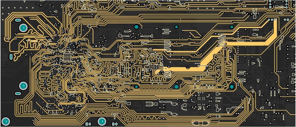
A printed circuit board, also known as the printed circuit board, printed circuit board, often using the English abbreviation PCB (Printed circuit board), is an important electronic component, is the support body of electronic components, and is the provider of electronic components line connection. It is made using electronic printing technology, called a “printed” circuit board.
What is PCBA?
PCBA (Printed Circuit Board Assembly) is a circuit board obtained by printing solder paste on the PCB and then installing various components such as resistors, integrated circuits, capacitors, and transformers according to the purpose and required characteristics of the board. PCBA is usually heated in a reflow oven to establish a mechanical connection between the PCB and the components.
The difference between PCB and PCBA
PCB is short for printed circuit board, an important electronic part for loading electronic components, and is the connection carrier for electronic component conduction. It is so-called because printing technology is used.
PCBs are divided by circuit layers into single, double-sided, and multi-layer. Typical are 4-layer and 6-layer multi-layer PCBs. More complex multi-layer PCBs have dozens of layers. They can also be divided into rigid, flexible, and rigid boards. Printed boards have developed from single-layer to double-sided, multi-layer, and flexible boards, maintaining their respective trends.
PCBA: Printed Circuit Board Assembly; circuit board assembly in the electronics processing industry mainly refers to various electronic parts, ICs, and other materials soldered or inserted on the blank circuit board and quality inspection and testing to ensure that it has complete circuit connection performance.
Blank boards are made according to customer PCB files. Therefore, the blank board has no electronic components, only a variety of pads. Install the electronic components on the PCB, the installation of electronic components is SMT processing, that is, electronic parts soldered on the pads, and then need to use DIP plug-in auxiliary processing to complete the entire welding process.
PCBA common processing equipment
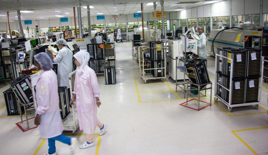
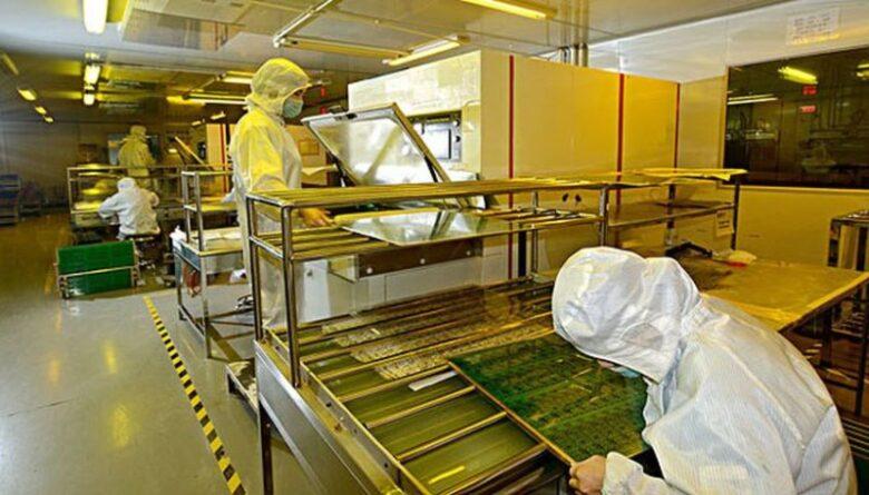
PCBA processing is a relatively high degree of integration of mechanical equipment, the electronic processing industry, more and more sophisticated processing machinery, and equipment use and manufacturing process improvements make PCBA processing yield of finished products continue to improve, and the efficiency gradually increased. pcba processing is commonly used in the following types of processing equipment.
PCBA processing equipment 1: printing machine
The printing machine is located in the front of the PCBA processing line; the main use is PCB circuit board printing solder paste or SMD adhesive. The workflow is the printing machine stencil mesh and PCB pads right, through the movement of the scraper, placed on the stencil of the solder paste or patch adhesive leakage printed on the PCB pads or the corresponding location, for PCBA processing of the subsequent process of component mounting to prepare.
PCBA processing equipment 2: dispensing machine
The main purpose of dispensing machine is to coat the solder paste or SMD adhesive. The workflow is to apply the formulated dose of glue or solder paste in the required position of PCBA devices through the pressure of the vacuum pump. The advantage of dispensing machine is that in the production process, there is no need to replace the production jig, which greatly shortens the production cycle and is suitable for small-batch multi-product production.
PCBA processing equipment 3: SMD machine
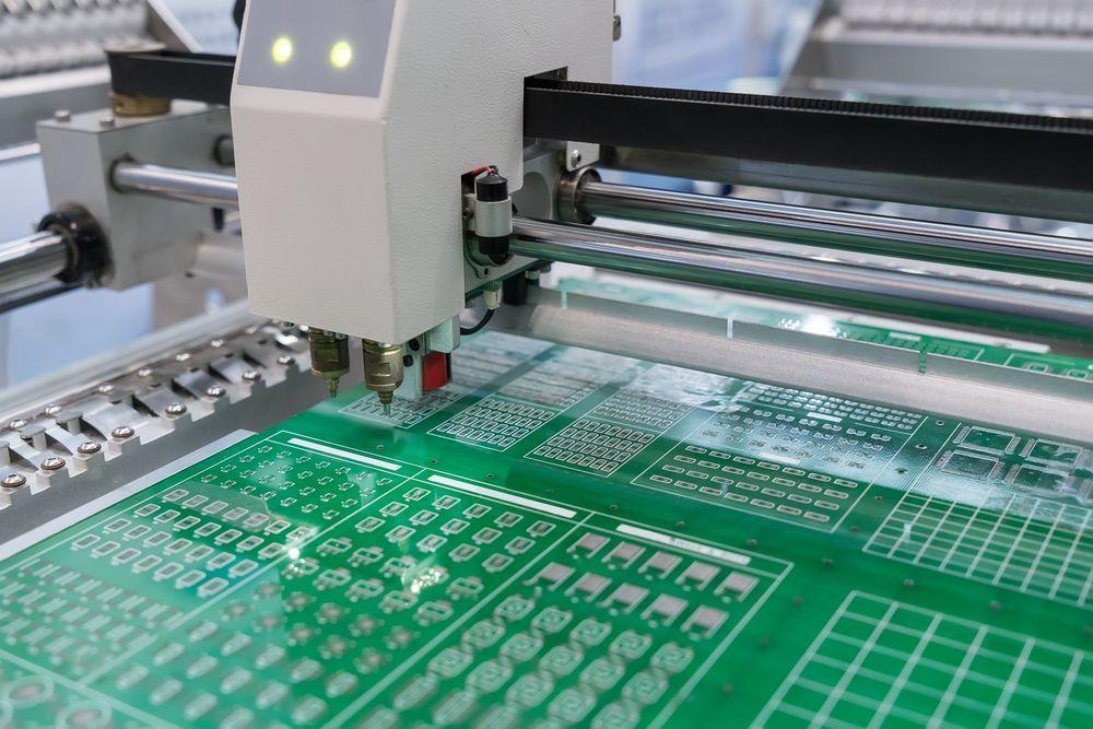
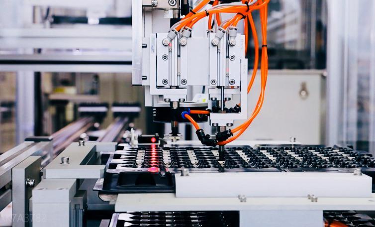
SMD machine is the core machinery and equipment in PCBA processing, also known as a mounting machine. The main use is through the pre-set conditions, accurate from the development of the location of the removal of know material, correctly affixed to the specified location. PCBA processing and production capacity depend mainly on the placement machine’s speed and accuracy and other functional parameters. It is also a PCBA process with the highest technical content and the most complex and expensive equipment.
An automatic bonder is a set of precision machinery, electric, pneumatic, optical, computer, sensing technology, Etc., as one of the high speed, high precision, highly automated, highly intelligent equipment.
PCBA processing equipment 4: reflow soldering machine
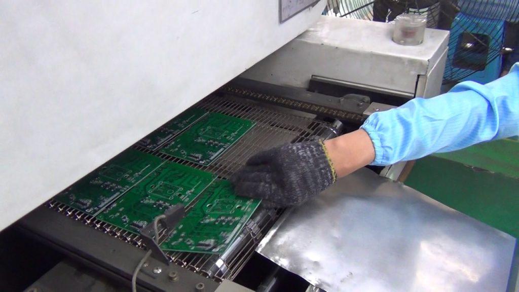
The main purpose is to fuse the solder pre-distributed by the printer on the PCB board by providing a stable and controlled heating environment so that the surface mount components and PCB pads are reliably bonded together through solder paste.
PCBA processing equipment 5: testing equipment
The main role of testing equipment is to assemble quality, and line street quality testing of the PCBA, which is well mounted, the equipment used mainly has a magnifying glass, microscope, automatic optical detector, online tester, X-ray testing system, and function tester. According to the needs of detection, its installation position is in the corresponding back position of the production line.
PCBA processing equipment 6: rework equipment
The main role of the reworked equipment is to detect the failure of the finished PCBA rework repair, the tools used for soldering iron, BGA rework table, Etc.
PCBA processing equipment 7: cleaning equipment
The role of cleaning equipment is to process the finished PCBA on the electrical properties of the material or harmful to human body soldering residues removed, such as flux, Etc. If you use no cleaning, solder can be used without cleaning, cleaning equipment used for ultrasonic cleaning machine and special cleaning liquid (washboard water: washboard water is an extremely volatile flammable liquid, pay attention to the use of safety).
PCBA processing process of the four major links
Circuit board to achieve functional operation, relying on a PCB bare board is unable to complete the need to bare board for component placement, plug-in, and welding; this step-by-step process is called PCBA. process PCBA process can be roughly divided into four main links, respectively: SMT chip processing → DIP plug-in processing → PCBA test → finished product assembly.
1. SMT chip processing link
SMT chip processing link will generally be based on the BOM list provided by the customer to match the purchase of components to confirm the production of the PMC plan. After the preparation work is completed, we will start SMT programming, making laser stencil and solder paste printing according to the SMT process.
Components are placed onto the board through the SMT placement machine, and online AOI automatic optical inspection is performed if necessary. After inspection, set the perfect reflow oven temperature profile and let the board flow through the reflow.
After the necessary IPQC mid-inspection, it is time to use the DIP plug-in process to pass the plug-in material through the board and flow through the wave soldering for soldering. Then comes the necessary post-oven process.
The above processes are completed, and QA for comprehensive testing to ensure product quality is passed.
2. DIP plug-in processing links
DIP plug-in processing process: plug-in → wave soldering → foot cutting → post-solder processing → wash board → quality inspection
3. PCBA testing
PCBA tests the entire PCBA processing process in the most critical quality control links; you must strictly follow the PCBA test standards by the customer’s test plan (Test Plan) on the board test points.
PCBA testing also contains five main forms: ICT testing, FCT testing, aging testing, fatigue testing, and testing under harsh environments.
4. Finished product assembly
The test OK PCBA board for the assembly of the shell, and then test, and finally can be shipped.
PCBA production is a chain of interlocking rings; any link problem will have a very big impact on the overall quality; there needs to be strict control of each process.
The above is about the PCBA process production of the four main links; each large link has countless small links to do auxiliary, and each small link will have a or some testing process to ensure product quality to avoid unqualified products in the factory.
PCB manufacturing of Anpllopcb
In today’s high-tech world, printed circuit boards are becoming more and more complex as technicians find ways to load more data and energy onto smaller and smaller chips. As computer equipment and electronic devices become smaller, the PCBs that power and connect them to the radio network will also become smaller. For PCB manufacturers, this means that the production of printed circuit boards will require advanced levels of engineering.
To increase the efficiency of PCB manufacturing to current standards, you must have properly specified bare PCBs to perform each step in the assembly process more efficiently. At Anpllopcb, we use the latest technology in our facilities to complete each bare PCB order to customer specifications. For more information on PCB manufacturing, please contact Anpllopcb.
Do you have questions about our services or your project? Contact us today to speak with Anpllopcb’s award-winning support team!

