- What is a Flex PCB?
- What is the Flex PCB prototype?
- The main components of the Flex PCB structure
- Design considerations for Flex PCBs
- Flex PCB Prototyping Tips
- Summary
In order to produce a Flex PCB prototype, there are several considerations related to the fabrication and end use of the Flex PCB circuit, including the design of the copper pattern itself. Before routing circuits in Flex PCBs, use the following design tips and considerations to maximize durability and yield. These tips can help you balance the durability of your Flex PCB prototype with the component layout and routing traces in your advanced PCB. Let us take a brief look at flex circuit prototyping.
What is a Flex PCB?
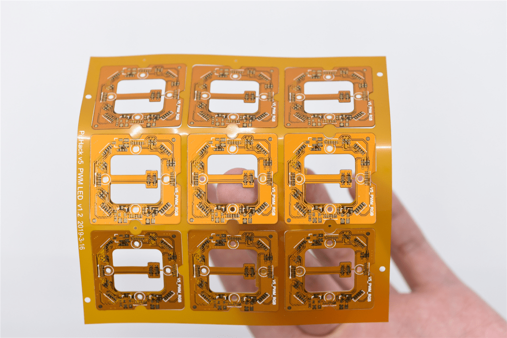
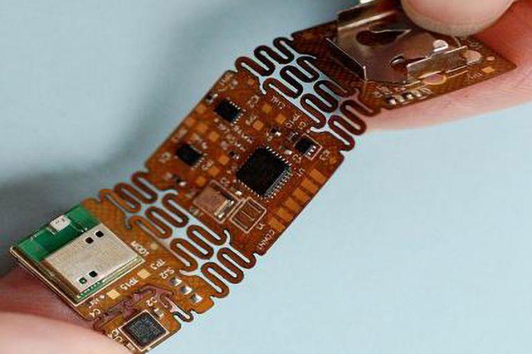
What is a flex PCB? In short, a flex PCB is a printed circuit board that uses bendable, durable, and Flex materials. It provides a lightweight, thin, Flex, and durable circuit board that is ideal for various applications. Most modern devices use Flex PCBs, from telecommunications to the aerospace industry. They use Flex PCBs as additional support for their motherboards to provide robust and stable connections for various components of their electronic devices.
Modern devices use Flex PCBs for a variety of purposes. For example, Flex circuit boards are used in most smartphones to connect the camera, battery, audio and various other modules to the motherboard. Flex PCBs make it easier to design compact products that offer users a wide range of features. In addition, Flex PCBs are very inexpensive to manufacture, which helps to reduce production costs while providing end users with a favourable product price.
What is the Flex PCB prototype?
A PCB (printed circuit board) prototype is a model or sample of how the final PCB will look and function. A printed circuit board prototype or low-cost PCB prototype is a small device used to connect electronic components to ensure the smooth operation of a product. The process determines whether the proposed PCB design will perform as expected, thus revealing any possible defects and thus allowing the designer to make any necessary changes. Any other improvements or alternatives the designer may have in mind are also introduced at this stage. Mass production of any new product is not possible without PCB prototyping services cannot simply start without a prototyping phase.
A Flex PCB is a special circuit board consisting of copper-metal traces combined with a dielectric layer such as polyimide. The circuit board can be bent into any desired shape, making it available for high-density applications. The Flex PCB concept originated in the 1900s and has enjoyed mainstream success due to its nearly limitless applications and possibilities.
Modern electronics would not be possible without using Flex PCB prototypes, including smartphones, computers, smart watches, keyboards, and various industrial applications that power technology.
The main components of the Flex PCB structure
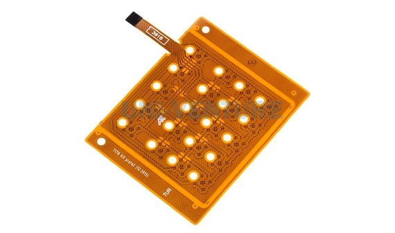
Flex PCBs may seem fragile and break down under heavy use, but their demand has skyrocketed due to their reliability and longevity. The main components of Flex PCBs are as follows.
Electrical conductors are made of copper, and traces are spread throughout the circuit.
Dielectric substrate film: This is the base material for Flex PCBs. Polyimide (PI) the most popular dielectric substrate film material is polyimide (PI) because of its temperature and traction resistance.
Adhesive material: Adhesives are used to join the different parts of the circuit together.
Protective coating: A thin coating of protective material applied to a Flex PCB. It is made of an overlay or cover layer.
Design considerations for Flex PCBs
Compared to rigid PCBs, Flex PCBs require a unique approach. The design process for Flex PCBs should result in significant savings in manufacturing costs, reduced weight and less space on the board. The board must be optimized for its application and materials.
A well-designed Flex PCB will be durable, easy for technicians to use, suitable for the intended use (such as a wearable device or computer, and light in weight.
The following points must be considered when designing your first flex PCB prototype.
Flex PCB bendability and flexibility
Your flex PCB will have varying degrees of flexibility depending on its application. You will need to know how many times it will bend and how severely it will bend. The number of times it can bend will play a role in determining whether the board is static or dynamic. Static boards are designed to be bent less than 100 times over their lifetime and considered bent for installation.
Due to their nature, dynamic boards have much greater design considerations. Dynamic boards need to be more robust because they are subject to more bending and need to withstand thousands of bends. These boards are suitable for applications without room for failures, such as military and spacecraft.
Flex PCB bending radius
The bend radius, also known as the minimum amount of flex in the Flex area of the circuit, must be determined at the earliest stages of a Flex PCB design. This will ensure that the design can accommodate a certain amount of bending without compromising the structural integrity of the copper. The standard minimum bend radius for Flex PCBs is ten times the thickness.
The following table shows the relationship between the number of layers and the bend radius.
| layers | Bending radius mm |
| one-sided | Bending thickness 6 |
| duality | Bending thickness 12 |
| multilayer | Bending thickness 24 |
Flex PCBs have thinner copper and insulation layers, occupying a minimal surface area and fitting into more compact spaces. Notably, 90-degree bending increases the chance of impedance discontinuities, which can affect functionality. For this reason, designers often avoid using plated through holes in the bend area.
Interleaved vias are a more desirable option when designing Flex PCBs because they ensure the longevity of the circuit in a multilayer circuit. Small conductors (less than 10 miles) are more suitable for neutral bending axes with no compression or tension during bending. This ensures that the characteristics of the circuit will not be affected when bending results in compression and tension.
Solder pads and over-hole placement
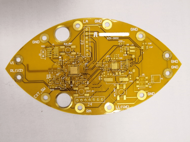
When designing a Flex PCB circuit, the focus should be on the bend. It is recommended that pads and vias not be placed within the bend area. Using teardrops on plated holes is also recommended to maximize durability and robustness. Flex PCB prototypes may be subject to different bending angles, so pads and vias should be much larger than drilled holes.
Wiring in Flex PCBs
A good rule of thumb when designing a Flex PCB is to ensure that the alignment is always routed at a 90-degree angle to bend the wires. If you are creating a board for high-speed signals (such as PCB bus routing), ensure that the top and bottom alignments are alternately interleaved and not overlapping.
This will distribute mechanical stress evenly across all traces. Flex PCB circuits should avoid all sharp corners (e.g., right angles). A better option is to use curves to maximize the life of the prototype.
Component Placement
It is recommended that low-frequency components be isolated from high-frequency components. This ensures that the high-frequency components do not interfere with the performance of the low-frequency components through noise induction. Doing so may affect signal quality, which is highly undesirable, especially in military applications.
It is recommended that clock signals be shielded using a material enclosure usually made of aluminium.
Flex PCB prototypes should be subjected to various tests before final use. The tests should check the Flex PCB’s basic performance and essential characteristics. The above tips should help designers to build a prototype with minimal errors. However, the perfect Flex PCB prototype depends on the application for which it is designed.
Flex PCB Prototyping Tips
Component placement needs to be given due attention. When circuits are bent, you need to pay special attention to spacing. Using 3D flex PCB design tools can go a long way to ensuring this. To prevent vias cracking, the vias must be torn out. In addition, the toroids need to be large no matter where the anchors or tabs are added. Due to the Flex nature of the circuit, the pad tends to lift off the substrate. Therefore, it needs to be anchored. This is accomplished by extending the tether from the pad of the overlay package. In addition, large pad sizes work well because they help relieve pressure. The pads must be larger than the drilled holes, as the prototype may bend at different angles.
Collation of issues to keep in mind when designing Flex PCB
(1) The alignment must be routed perpendicular to the bending line.
(2) Mechanical stress needs to be evenly distributed over all alignments.
(3) large bending radius than the sharp corner effect is much better. A bent alignment produces lower stress than an angled alignment. In addition, the alignment should remain perpendicular to the entire bend.
(4) Shaded polygons in the ground plane work better than solid-filled polygon planes. Using shaded polygons, the risk of copper cracking is significantly reduced.
(5) Flex layers should be placed in the centre of the stack. By doing this, you tend to protect yourself from exposure to the outer plating. It also simplifies manufacturing and improves impedance.
(6) We Need to consider factors such as the bend radius size to determine the material’s thickness. As a rule of thumb, the bending radius of a Flex PCB should not exceed 10 times its thickness.
(7) When it comes to Flex circuits, impedance control is challenging. Single-layer Flex circuits can use a coplanar ribbon line structure. A two-layer flex stack would benefit from a microstrip structure suitable for 50-ohm circuits. With higher layer counts, you can create ribbon line structures.
Pitfalls to avoid in the design phase when it comes to Flex PCBs
(1) Considering bending at the end of the assembly instead of the beginning can lead to many problems, including creating more expensive bends.
(2) Designs that do not consider manufacturability practices can lead to costly mistakes. Factors such as minimum wire width/spacing toroids must include manufacturing allowances in the CAD design.
(3) Failure to consider the possible effects of different tolerances. Many times, the design does not take into account the realities of the material. For example, hole pattern locations can inhibit bending.
(4) Not-sequenced documents can also lead to many problems. Whether it is creating a comprehensive drawing package or not or incorrect revision control, it can have an impact.
(5) Electrical and mechanical design issues also need to be considered. Some of these include considering the number of bends and balancing electrical and mechanical requirements. For example, high-speed signals require thick substrates. Likewise, high current layers require thicker foils and adhesives.
(6) It is also important to consider cost drivers (e.g. number of layers). In addition, slight adjustments in shape can lead to cost differences, especially for larger circuits.
Summary
This article summarizes tips on Flex PCB design and considerations if the time comes to develop a new Flex PCB. PCB prototyping services designers should always be prepared for any upcoming possible results. While the PCB is still in the prototype verification stage, any rework should not be considered an additional cost. Bypassing prototyping and going straight to mass production of PCB prototype boards will only lead to project failure and can be catastrophic for any company.
Anpllopcb providing some of the most innovative printed circuit board technologies and highest quality standards in the industry. You can count on us to meet your needs, from the simplest boards to the most complex designs for small quantity and large scale production.

