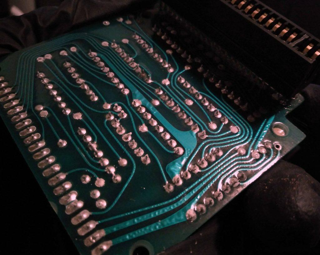
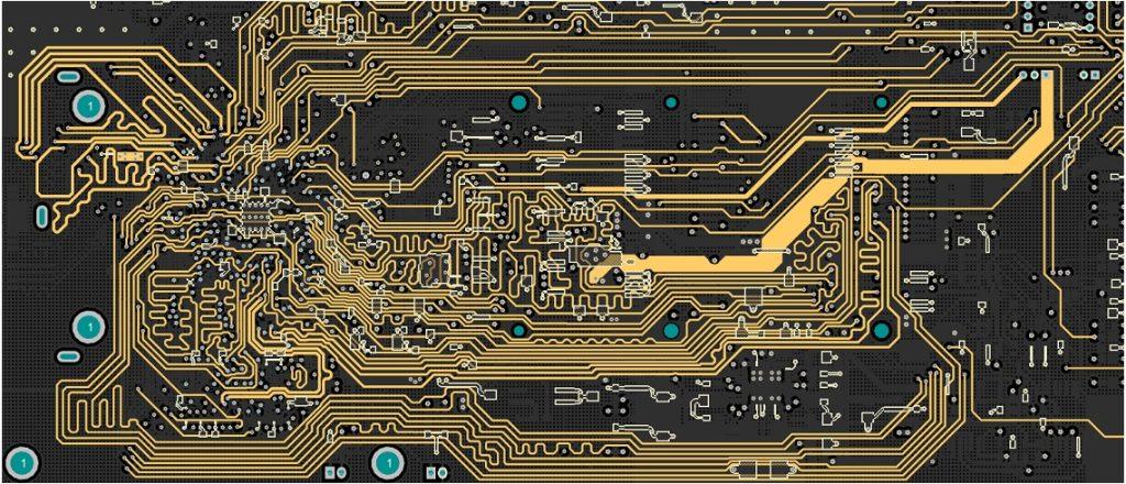
- What is printed circuit board soldering?
- Printed circuit board soldering skills
- Printed circuit board welding precautions
- Double-sided printed circuit board characteristics
- Double-sided printed circuit board welding method
What is printed circuit board soldering?
What is printed circuit board soldering? Printed circuit board soldering is the process of soldering components to a PCB printed circuit board (bare board). In recent years, the electronics industry process development history PCB soldering technology in recent years, you can notice a very obvious trend in reflow soldering technology. In principle, conventional cartridges are also available for the reflow soldering process, which is commonly referred to as through-hole reflow soldering. The advantage is that it is possible to complete all solder joints simultaneously, keeping production costs to a minimum. Temperature-sensitive components, however, limit the application of reflow soldering, both cartridge, and SMD.
Selective soldering can be used in most applications after reflow soldering. This will become an economical and efficient way to complete the remaining cartridge soldering method and is fully compatible with the future of lead-free soldering.
Printed circuit board soldering is divided into straight insert soldering and SMD parts soldering.
Pcb straight plug-in welding generally has soldering iron welding method, dip soldering method, and wave soldering method three; PCB manufacturers will use different welding methods according to different production needs. PCB production and processing plant in the daily production needs will use the following PCB welding methods:
1. sample and small quantities of the general use of manual soldering iron welding method.
2. Small batch of the general use of dip welding method.
3. Large quantities of general use of wave soldering method.
4. SMD welding generally has soldering iron soldering and reflow soldering methods.
5. sample and simple boards generally use the soldering iron welding method.
6. Complex boards and large quantities of general use of reflow soldering method.

Printed circuit board soldering skills
1, selective soldering process includes: flux spraying, board preheating, dip soldering and drag welding. The flux coating process in the selective soldering flux coating process plays an important role.
The flux should be active enough to prevent bridging and oxidation of the board at the end of the heating and soldering process. Flux spraying by X / Y robot carrying the board through the flux nozzle above, flux spraying to the PCB board soldering position.
2, reflow process after the microwave peak selection of welding, it is important that the flux is accurately sprayed, micro-hole spray type will not get dirty outside the area of the solder joint.
Micro-spot sprays flux point graphics diameter is greater than 2mm, so spray deposited on the circuit board flux position accuracy of ± 0.5mm to ensure that the flux always covers the top of the soldered parts.
3, can be compared with wave soldering to understand the process characteristics of selective soldering; the obvious difference between the two is that the wave soldering in the lower part of the printed circuit board is completely immersed in liquid solder, while in selective soldering, only some specific areas in contact with the solder wave.
Since the printed circuit board is a poor heat transfer medium, it does not heat up. During soldering, it melts the solder joints of adjacent components and printed circuit board areas.
Before soldering must also be pre-applied flux; compared with wave soldering, flux is only coated in the lower part of the board to be soldered rather than the entire PCB board.
In addition, selective soldering is only applicable to the soldering of cartridge components. Selective soldering is a completely new method. A thorough understanding of the selective soldering process and equipment is necessary for successful soldering.
Printed circuit board welding precautions
1, remind you to get the PCB bare board should first be checked for appearance to see if there is a short circuit, broken circuit, and other problems, and then become familiar with the development board schematic diagram, the schematic diagram and PCB screen printing layer for comparison, to avoid schematic diagrams and PCB does not match.
2, PCB welding required materials are ready; the components should be classified into several categories according to the size of all components to facilitate subsequent welding. Need to print a complete list of materials. Do not finish welding one in the welding process, then use a pen to cross out the corresponding options to facilitate subsequent welding operations.
3, before welding, should be taken to wear a static electricity ring and other anti-static measures to avoid electrostatic damage to components. After the equipment required for welding is ready, you should ensure that the soldering iron head is clean and tidy. The first welding recommended the use of flat-angle soldering iron; in welding components, such as 0603 type package, a soldering iron can better contact the pad, easy to weld. Of course, for masters, this is not a problem.
4, the selection of components for welding should be by the components from low to high, from small to large order welding. Avoid welding the larger components to the smaller components of the welding inconvenience. Priority welding integrated circuit chips.
5, integrated circuit chip welding before the need to ensure that the chip is placed in the correct direction. For the chip screen printing layer, the general rectangular pad indicates the beginning of the pin. Welding should be fixed first, chip a pin, and the location of the components for fine-tuning after fixing the diagonal chip pins so that components are accurately connected to the location after welding.
6, chip ceramic capacitors, voltage regulator circuits in the voltage regulator diode without positive and negative, light-emitting diodes, tantalum capacitors, and electrolytic capacitors must distinguish between positive and negative. Capacity and diode components generally have a sign marking end that should be negative. In the SMD LED package, the direction of the light is positive-negative. For silkscreen marking for the diode circuit diagram package components, a vertical line end should be placed on the negative end of the diode.
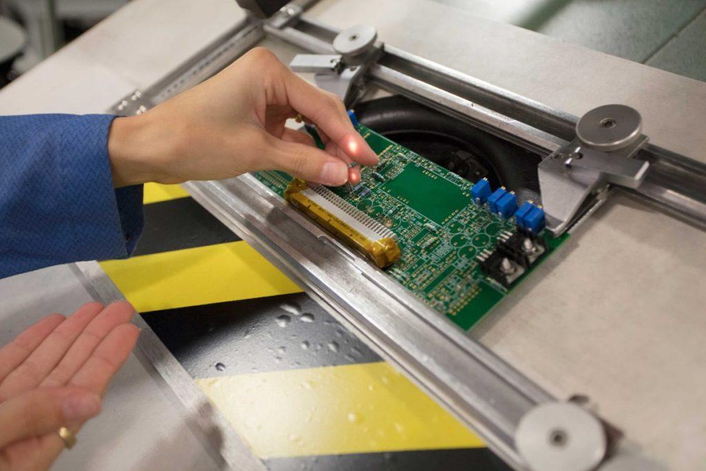
7, for the crystal, passive crystal generally has only two pins and no positive or negative. Active crystal generally has four pins; you need to pay attention to the definition of each pin to avoid welding errors.
8, for the welding of plug-in components, such as power module-related components, the device pins can be modified before welding. After the components are placed and fixed, generally on the back, the soldering iron will melt the solder by the pad into the front. The solder does not have to put too much but first should make the components stable.
9, the welding process should be recorded promptly found. For subsequent improvement, PCB design problems, such as mounting interference, incorrect pad size design, component packaging errors, Etc., for subsequent improvement.
10, after welding completion, a magnifying glass should be used to view the solder joints, check whether there is a false solder and short circuit, Etc.
11, PCB circuit board soldering work is complete should use alcohol and other cleaning agents on the surface of the circuit board for cleaning to prevent the circuit board surface from attaching to the iron chips to short circuit, but also to make the circuit board more clean and beautiful.
Double-sided printed circuit board characteristics
The difference between single-sided and double-sided printed circuit boards is that the number of layers of copper is different. A double-sided printed circuit board is a printed circuit board on both sides of the copper; you can play a role in the connection through the hole conductivity. Single-sided, only one layer of copper, only a simple line, the holes made can only be used for plug-in and can not conduct.
The technical requirements of the double-sided printed circuit board are the wiring density, smaller hole diameter, and metalized hole aperture also getting smaller. Layer and layer interconnection rely on the metallization hole, the quality directly related to the reliability of the printed circuit board.
With the reduction of the aperture, the original to the larger aperture did not affect the debris, such as grinding debris, once residual in the small hole inside, will make the chemical precipitation copper, copper plating to lose effect, the hole without copper, become a hole metallization of the fatal killer.
Double-sided printed circuit board welding method
Double-sided printed circuit board in order to ensure that the double-sided circuit has a reliable conductive effect, PCB welding should first use wires and such to weld the connection hole on the double-sided panel (i.e., the metalization process through the hole part) and cut off the connection line tip protruding part, so as not to stab the operator’s hand, which is the board’s connection preparation work.
Double-sided printed circuit board welding essentials.
1, there is a requirement for the shaping of the device should be processed by the requirements of the process drawings; that is, first shaping after the plug-in.
2, after shaping the diode model side should face up; there should be no inconsistency in the length of the two pins.
3, the device with polarity requirements, when inserted to pay attention to its polarity, shall not be inserted in reverse, roll integrated block components; after inserting, whether the vertical or lying device, there shall be no obvious tilt.
4, soldering iron power of 25 to 40W, soldering iron head temperature should be controlled at about 242 ℃; if the temperature is too high head easily “dead”; the low temperature can not melt the solder, soldering time control in 3 to 4 seconds.
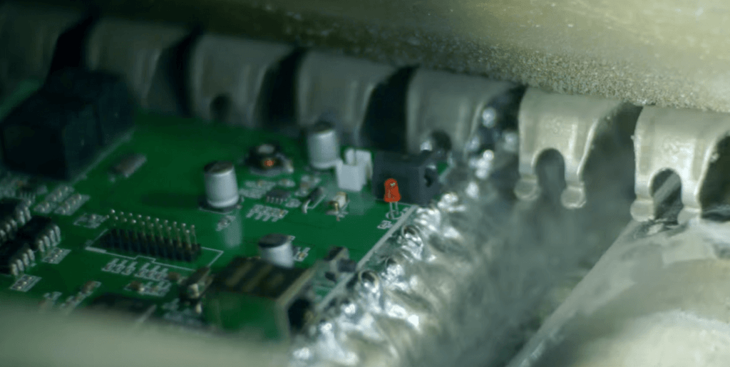
5, proper welding by the general device from short to high, from the inside to the outside of the welding principle to operate, welding time to master, too long will burn the device, will also burn the copper clad lines on the copper clad board.
6, because it is double-sided welding, so should also place the circuit board frame and so on; the purpose is not to press the oblique below the device.
7, after the completion of the circuit board soldering, should be a comprehensive check on the number of the type, check the place where there is a leak of insertion and leakage of welding to confirm the circuit board redundant devices such as pin trimming, after flowing into the next process.
8, in the specific operation, should also strictly follow the relevant process standards to ensure the quality of the product welding.
With the rapid development of high-tech and the public’s close relationship with electronic products in the continuous renewal, the public also needs high-performance, small-size, multi-functional electronic products, which puts forward new requirements for printed circuit boards.
The double-sided printed circuit board was therefore born due to the widespread use of double-sided printed circuit board, prompting the printed circuit board manufacturing to light, thin, short, and small development.

