- (1) What is PCB reflow soldering?
- (2) What is PCB laser welding?
- (3) printed circuit board (PCB) welding precautions
- (4) Summary
With all kinds of electronic products beginning to miniaturize, the traditional PCB welding technology in a variety of new electronic components on the application of a certain test. In order to meet such market demand in the PCB welding process technology, it can be said that the technology is constantly improving, and PCB welding methods are also more diverse. This paper selects the PCB traditional welding method reflow soldering and innovative PCB laser welding method for comparison; you can more clearly see the technical innovation to bring convenience.
(1) What is PCB reflow soldering?
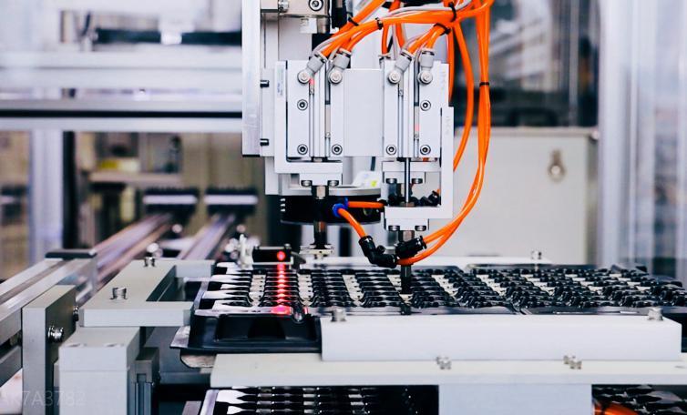
Pcb soldering process reflow soldering and traditional wave soldering, the most obvious difference between the two is that the lower part of the traditional PCB wave soldering PCB completely immersed in liquid solder, while in PCB reflow soldering, only some specific areas in contact with the solder. During the soldering process, the position of the solder head is fixed, and the PCB is driven in all directions by a robot. Flux must also be pre-applied before soldering. Compared with PCB wave soldering, flux is applied only to the lower part of the PCB to be soldered rather than the entire PCB.
Pcb reflow soldering uses a pattern of applying flux first, then preheating the board/activating the flux, and then using a soldering nozzle. The traditional manual soldering iron requires point-to-point soldering for each point of the board, so there are more soldering operators. The choice of PCB wave soldering is an industrialized mass production mode in an assembly line, where different-sized soldering nozzles can be used for batch soldering, usually increasing the soldering efficiency by more than a few dozen times compared to manual soldering (depending on the specific board design). Thanks to the small programmable mobile soldering cylinders and various flexible soldering nozzles (the capacity of the cylinders is about 11 kg), it can be programmed to avoid certain fixed screws and reinforcements under the circuit board to avoid damage caused by their contact with high-temperature solder. Such a PCB soldering mode, without needing custom soldering trays and other methods, is ideal for multi-species, low-volume production methods.
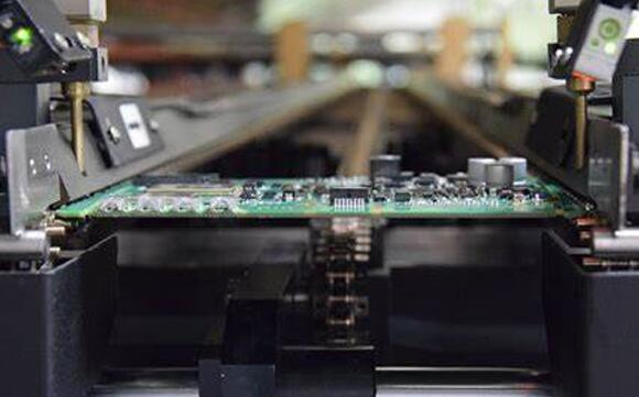
①Line board reflow soldering process features
1、The size of the solder joint can be controlled. Can be designed by the size of the pad and the amount of printed solder paste to obtain the desired solder joint size or shape requirements;
2, solder paste is generally used in the stencil printing method to simplify the process and reduce production costs. Usually, each solder surface is only once printed solder paste. This feature requires that each assembly surface component can use a stencil (including the same thickness stencil and step stencil) for solder paste distribution;
3, PCB reflow oven is a multi-temperature tunnel oven; the main function is to heat the PCBA. The layout on the bottom side (B side) of the components should meet the fixed mechanical requirements, such as BGA class package, component quality and pin contact area ratio ≤ 0.05mg/mm2 requirements, in case the top surface components do not fall off when welding;
4, PCB reflow soldering, the components are completely floating on the molten solder (solder joints). If the pad size is greater than the pin size, the component layout is heavy, and the pin layout is less, it is easy to shift in the asymmetric molten solder surface tension or reflow soldering furnace forced convection hot air blowing;
5, in general, the ability to correct the position of their components, pad size and solder end or pin overlap area of the larger the ratio, the stronger the positioning function of the components. We are using this point to have the positioning requirements of the components of the specific design of the pads;
6, the solder seam (point) shape formation depends mainly on the molten solder’s wetting ability and surface tension’s role, such as 0.44mm QFP and printed solder paste graphics for the regular rectangular shape.
② The advantages of reflow soldering in the soldering of through-hole component boards
● High productivity in soldering and a high degree of automation in soldering
● Precise control of flux injection position, injection volume, microwave peak height, and soldering position
● Nitrogen protection of the microwave peak surface; optimization of process parameters for each solder joint
● Quick change of nozzles of different sizes
● Combined technology for spot welding of individual joints and sequential row welding of through-hole connector pins
● Fat” and “thin” joint shapes can be set according to requirements
● Various preheat modules (infrared, hot air) and additional preheat modules on top of the board are available
● Maintenance-free electromagnetic pump
● The choice of construction materials is perfectly suited for lead-free solder applications
● Modular structure design reduces maintenance time
(2) What is PCB laser welding?
The light source for PCB laser welding is a laser light-emitting diode, which can be precisely focused on the solder joint through an optical system. PCB laser welding has the advantage that the energy required for welding can be precisely controlled and optimized. It is suitable for selective reflow processes or connectors with solder wire. In the case of SMD components, the solder paste is first applied and then soldered. The soldering process is divided into two steps: First, the paste is heated, and the solder joint is preheated. The solder paste is then completely melted, and the solder completely wets the pad, resulting in a solder. Using the laser generator and optical focus assembly welding, high energy density, high heat transfer efficiency, and non-contact welding, solder can be solder paste or wire, especially suitable for welding small space solder joints or solder joints short power, energy saving.
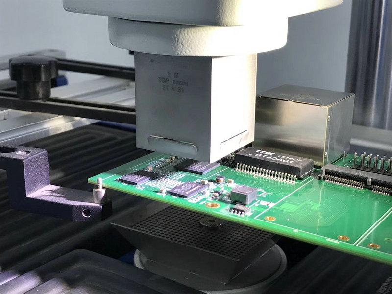
① Pcb laser welding features
●Multi-axis servo motor board control, high positioning accuracy
●Laser spot is small and has obvious welding advantages on small-size pads and pitch devices
●Non-contact welding, no mechanical stress, static electricity risk
●No dross, less flux waste, low production cost
●Various types of products that can be soldered
●Many choices of solder
②Laser welding of PCB board through-hole pads
In order to meet such market demand, it can be said that the welding process technology is constantly improving the technology; welding methods are also more diversified, including PCB through-hole components of the laser in welding technology innovation, to PCB manufacturing companies to bring efficient production.
The advantage of laser soldering of PCB through-hole components is that it can precisely control and optimize the energy required for welding. Solder is applied by spot coating the solder paste and then soldering. The solder completely wets the pad, resulting in a rounded, full, uneven solder joint. Using laser generator and optical focus assembly welding, high energy density, high efficiency of heat transfer, non-contact welding, solder can be solder paste or tin wire, especially suitable for welding solder joints or small solder joints in a narrow space, low power, energy saving, PCB board through-hole components through the tin rate of up to 100%, which is difficult to achieve the advantages of the traditional PCB soldering process.
③ Pcb laser welding advantages
For ultra-small electronic substrates and multi-layered electrical parts, the “traditional process” is no longer applicable, which has led to rapid technological progress. The processing of ultra-small parts unsuitable for the traditional soldering iron method is finally accomplished by PCB laser welding. “Non-contact welding” is the biggest advantage of laser welding. There is no need to touch the substrate or the electronic components, and providing solder by laser light alone does not cause a physical burden. Effective heating with a blue laser beam is also a major advantage. It can irradiate narrow areas inaccessible to the soldering iron tip and change angles when there is no distance between adjacent components in a dense assembly. The soldering iron tip needs to be replaced regularly, while laser welding requires few replacement parts and low maintenance costs.
The technical advantages of laser welding PCB through-hole pads:
1. laser soldering equipment using multi-axis servo motor board control + CCD vision, high accuracy of motion positioning.
2. small laser spot, pads, and small pitch devices welding has advantages.
3. non-contact welding, no mechanical stress, static electricity risk.
4. No tin slag or flux waste; the welding process will not cause fried tin, even tin and other undesirable phenomena, and low production costs.
5. can be soldered product type rich, through-hole pin parts welding through the high rate of tin.
6. Laser soldering selection (solder paste, wire, tin balls, Etc. optional).
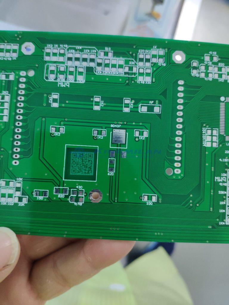
(3) printed circuit board (PCB) welding precautions
1, the printed circuit board holding method and the identification of the front and back of the PCB with your hands, you should take the corners or edges of the PCB to avoid bare-hand contact with the board’s solder joints, components and connectors.
(1) hands of oil and stains will hinder the smooth soldering.
(2) around the solder joints will be oxidized, the outermost layer will be damaged, and fingerprints on components, solder joints risk corrosion.
2, in the circuit board welding and device pick-up process, we need to wear anti-static wrist guards to perform anti-static protection measures and to ensure the effectiveness of anti-static wrist guards’ grounding.
(4) Summary
PCB soldering technology in recent years, the electronics industry process development process, it can be noted that a very obvious trend is PCB reflow soldering technology. In principle, the traditional cartridge is also available PCB reflow soldering process, commonly referred to as through-hole reflow soldering. The advantage is that it is possible to complete all solder joints simultaneously, keeping production costs to a minimum. However, temperature-sensitive components limit the application of reflow soldering, both for cartridges and SMDs. Laser selective soldering can be used in most applications after PCB reflow soldering. This will be an economical and efficient way to complete the remaining cartridge PCB soldering and is fully compatible with future lead-free soldering.
Anpllopcb offers some of the industry’s most innovative PCB technology and the highest quality standards. You can count on us to meet your needs, from the simplest circuit boards to the most complex low-volume and mass-production designs.


