OUR SERVICES
Manufacturing Multilayer PCBs
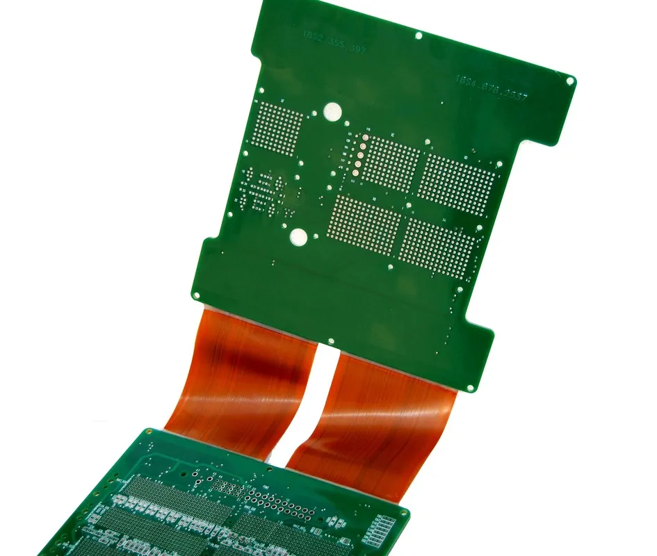
Anpllopcb manufactures multilayer PCB up to 56 Layers, accepting pure single or mixed-press materials: Fr4, Rogers, Polymide, and metal Core.
Multilayer PCB Manufacturer
We specialize in the design and production of multilayer printed circuit boards. If you need your PCBs in hand as fast as possible, you can trust Anpllopcb.
Our highly trained assembly technicians specialize in multilayer circuit boards. They use state-of-the-art multilayer circuit board fabrication equipment to ensure that the finished boards we distribute meet your exacting standards and technical specifications. You will also find that our multilayer PCB price fits your project budget.
Same-day turnaround is available on two-layer PCBs, and 24-hour turnaround is available on multilayer circuit boards. Despite our incredibly quick turnaround, our company takes no shortcuts in fabricating multilayer PCBs. The multilayer PCB fabrication process requires more attention to detail than the average printed circuit board. Care must be taken to ensure all layers are correctly registered despite deformations and stresses from the heat and pressure of the multilayer PCB manufacturing process.
Anpllopcb is the company to turn to for multilayer PCB design and multilayer PCB board fabrication that meets your project demands. If you’re waiting on multilayer PCBs to bring your product to market, we can help. To minimize the cost and turn of your PCB order, we recommend you speak with one of our PCB design and manufacturing experts. Our experts can consult with you about the design and specifications of your multilayer circuit board to achieve the capabilities, performance, and cost you are expecting.
contact us
Multilayer PCBs, Multilayer Boards (MLB) Services
The demand for multilayer printed circuit boards has been on the rise. The drive for electronics to be smaller, faster, and more powerful has made the multilayer PCB much more popular. The ability to create multilayer boards opens up a world of possibilities allowing the engineer to create more densely populated circuit boards which allows miniaturization. This is a huge benefit that double-sided boards are not able to offer.

HOW ARE MULTILAYER PCBS MADE?
Alternating layers of prepreg and core materials are laminated together under high temperatures and pressure to produce Multilayer PCBs. This process ensures that air isn’t trapped between layers, conductors are completely encapsulated by resin, and the adhesive that holds the layers together is properly melted and cured. The range of material combinations is extensive, from basic epoxy glass to exotic ceramic or Teflon materials.
The prepper and core are essentially the same material, but the prepreg is not fully cured, making it more malleable than the core. The alternating layers are then placed into a lamination press. Extremely high temperatures and pressures are applied to the stackup, causing the prepreg to “melt” and join the layers together. After cooling off, the result is a very hard and solid multilayer board.
Steps of Multilayer PCB Manufacturing
Plan the layout PCB design following all the requirements and encode it. By doing this, you are making sure that the different aspects and parts of the designs are error-free. A completed PCB design is then ready for fabrication building.
As soon as the check completion is finalized on the design, it can be printed. You punch the registration hole to serve as a guide for aligning the films as you continue with the process.
This step is the first while making the inner layer of the PCB. You print the multilayer PCB design; then, copper is re-bonded to the lamine piece that serves as the PCB structure.
The copper the photoresist does not cover is removed with a strong and effective chemical. As soon as it is removed, it leaves just the needed copper for your PCB.
Once the layers are free from defects, then you can fuse them. You can achieve this process in two steps: the lay-up and the laminating step.
Before you drill, the drill spot is located with an x-ray machine. This helps in securing the PCB stack.
This process helps in fusing the different PCB layers using a chemical.
By doing this, you guard the copper found on the outer layer by applying the photoresist.
To protect the copper during the process, a tin guard is utilized. This gets rid of unwanted copper. This also ensures properly established PCB connections.
After cleaning the PCB panels, apply an ink epoxy with a solder mask.
PCB plating is done to ensure that the components’ soldering can be achieved. The process of screening points out all the important information on the PCB.
To ensure functionality, the technician tests several areas of the PCB.
Different PCBs are cut from the initial panel according to the customer’s requirements. Then the board inspection is done, and the errors are rectified before it is sent for delivery.
BENEFITS OF MULTILAYER PCBS
- Higher assembly density
- The smaller size (considerable savings on space)
- Increased flexibility
- Easier incorporation of controlled impedance features.
- EMI shielding through careful placement of power and ground layers.
- Reduces the need for interconnection wiring harnesses (reduces overall weight)
Choosing the Right Vendor for Multilayer PCBs
The processes to manufacture multilayer printed circuit boards require specialized equipment and a significant commitment to operator training, not to mention financial consideration. This explains why some fabricators have been slower to enter the multilayer manufacturing market than others. Anpllopcb can provide expanded capabilities to support advanced printed circuit board designs with demanding requirements, including laser-drilled microvias, cavity boards, heavy copper up to 20 oz., via-in-pad, microwave & RF boards, up to 40 layers, and others.
We Want To Work With You!
Get an Instant Quote to Compare Price & Turn Times Side-by-Side.We make it a point to make sure that what we deliver is exactly what you want.
