This article describes how best to prepare your PCB design for manufacturing and assembly.
This is a common situation: you are a hardware developer with a looming deadline for your next product. A bad prototype PCB will delay the project by weeks, and you need to mitigate that risk. It is critical to assemble the PCB correctly the first time, quickly, and without problems.
To minimize these potential problems, Anpllopcb has compiled a list of tips to help you prepare your next prototype for manufacturing.
- Double-check the footprint and packaging
- Select a large number of tested part replacements
- Utilize pre-certified radio modules
- Consider your wireless antenna layout.
- Do not forget to decoupling capacitors.
- Protect your board with proper alignment width and spacing
- Choosing the right power regulator routing
- Using Linear Regulators
- Use switching regulators
- Includes large copper traces and heat release for potting
- Optimize your SMT assembly design
- Double-check your design rules check
- PCB Solution Provider
Double-check the footprint and packaging
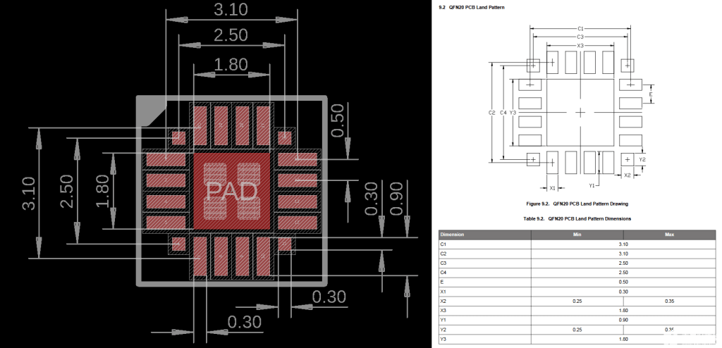
Ensuring the packaging matches the component is the first way to avoid manufacturing hang-ups. Considering how small some components have become and package contacts like BGA components, the old-fashioned method of printing out your PCB on paper at a 1:1 ratio and then covering your parts goes so far.
Double-check that the dimensions on the package match your design’s units (mm or mil).
Some component manufacturers are unfriendly and draw the mechanical layout of the component as a transparent PCB viewed from the bottom. Be sure to note this.

Figure 1. Silicon Labs EFM8UB10F8G in QFN20 package. Compare the layout drawn in the EDA tool with the landing pattern in the datasheet.
If your EDA tool can draw projection and dimension lines, it may be worthwhile to measure your footprint in a way that matches the mechanical drawing in the component datasheet. Verify the units of measurement of the data sheet and your footprint.
This is also a good time to check the mapping between schematic symbols and component packages. Voltage regulator lead wires, discrete MOSFETs, and transistors are often easily flipped.
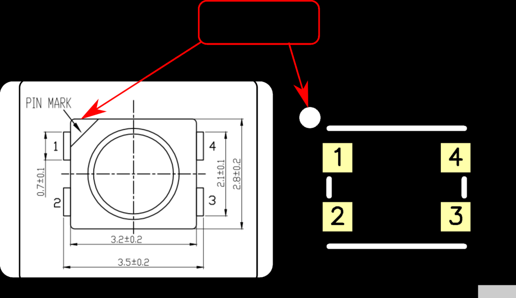
Components with polarities should check their packages to ensure that the polarity markings are marked. This includes IC pin one markings, diode cathode markings, and polarization capacitor markings.

Figure 2. Marking of pin 1 on a CREE LED.
Select a large number of tested part replacements
Production delays often occur when critical parts are unavailable, and there are no pre-tested and approved replacements. Suppose a part has viable alternatives but is in the critical path of a circuit or product. In that case, I strongly recommend you build prototypes and test each alternative before going into production. This reduces the risk of switching to an alternative part in the future.

Figure 3. End-of-life parts marked as NRND or not recommended for new designs on Mouser
If you have any unique parts that are not direct replacements (microcontrollers, specialized sensors, etc.), check the part life at the time the part was manufactured. Manufacturers will mark components scheduled for discontinuation as “Not Recommended for New Designs.”
Typically, manufacturers guarantee a fixed life for manufactured parts and notify users at end-of-life (EOL). Ensure that the needed parts are available until the end of the product’s production life to help prevent costly product redesigns.
Utilize pre-certified radio modules
Consider using a pre-certified radio module if your product uses Bluetooth or WiFi. These modules are pre-engineered and packaged systems guaranteed to operate correctly with the associated FCC identification number. Using pre-certified radio modules increases the chances of a properly functioning wireless system and reduces the likelihood of failing FCC and CE radio emission compliance testing.
Consider your wireless antenna layout.
The PCB layout of the antenna is critical if you believe the cost savings of rolling the wireless connection on the PCB is worth it. For most wireless connectivity components (transceivers), the manufacturer’s data sheet will have a recommended layout.
There are a few things to remember when doing the PCB layout. First, the impedance between the transceiver and the antenna must match. Second, the datasheet for the transceiver should contain more detailed information about choosing the right antenna, designing the tuning filter, and the correct impedance needed for optimal performance.
If you are designing your wireless connection, I strongly recommend performing pre-compliance testing on your product. Pre-compliance testing is expected to uncover any obvious problems with your design. Look for frequency harmonics in the target range in the clock, oscillator, and transmission spectrum.
Do not forget to decoupling capacitors.
Electrical components require a stable voltage source, and decoupling capacitors should be installed close to each active component on the PCB. Decoupling capacitors work best when placed close to the component’s power supply pins.
For larger components with multiple power pins, you may need to use decoupling capacitors at each power pin. Power-sensitive components such as sensors, ADCs, and FPGAs may also require decoupling capacitors, including a ground pin. The decoupling capacitors should be connected in series with the power supply and the component, as this improves the performance of the capacitors.
Protect your board with proper alignment width and spacing
High current alignments must be properly sized to ensure that they do not burn up your PCB, and I recommend using an in-line alignment width calculator for this calculation. Alignments on the outside of the board can handle more current than the inside because the outside alignments are more likely to dissipate the heat generated. To reduce the heat, try specifying a temperature rise of 10C on the trace width calculator, but if you do not have enough room for such a wide trace, then a 20ºC temperature rise should be fine for most applications.
If you cannot route the traces wide enough, you may need to use a thicker copper weight, increasing the current capacity. However, increasing the copper weight thickness may cause Design Rule Check (DRC) issues with minimum alignment width and spacing, so consider this. Often thickening with increasing copper weight will require greater alignment width and space and increase the price per PCB unit.
An issue often overlooked is ensuring that high-voltage traces are adequately isolated from each other. If your product is connected to a supply voltage, you must ensure the voltage does not cross the air gap and short out.
Choosing the right power regulator routing
There are two main voltage regulators in embedded systems: linear and switching. Each type has different PCB layouts and wiring guidelines.
Using Linear Regulators
Linear regulators absorb excess voltage and convert it to waste heat. It is inefficient, but linear regulators usually require only external capacitors to operate properly and are less noisy than switching regulators. There are two things to ensure the proper use of linear regulators.
Consider your choice of capacitors. Follow the manufacturer’s guidelines for the capacitors’ type, value, and location to bypass the regulator. In general, capacitors should be located as close as possible to the input and output pins of the regulator.
Take care of the heat. In general, this means ensuring that the package you choose for your regulator can handle the heat you generate and that your layout can support it. Copper potting and stitching through will be your friend. You will need a heat sink if the copper pour is not large enough.
Use switching regulators
Switching regulators are more efficient than linear regulators but more complicated to design. Switching regulators do not have heat problems, but you must choose components carefully to ensure the switching regulator works properly. Switching regulators are also more likely to generate unwanted electromagnetic fields (EMFs) and cause products to fail during the FCC/CE compliance phase.
Strictly follow the manufacturer’s recommended layouts. These layouts have been tested and work properly.
Keep the feedback loop of the switcher as small as possible. This will reduce EMF and parasitic resistance, inductance, and capacitance.
Pay close attention to the ESR and ESL ratings of your switching regulator output capacitors. When looking for components, the data sheets for switching regulators will usually tell you where to set the values.
For designing switchers, use Texas Instruments Webench. It generates multiple designs for the specifications and gives you the part numbers for the inductors and capacitors you need to design your switchers properly.
Includes large copper traces and heat release for potting
Copper solder pads with heat release can be created by connecting pads to copper traces or using smaller narrow traces instead of direct connections for potting. Heat release reduces the heat load of soldering the component to the pad. Since copper dissipates heat quickly, this reduces the chance of cold solder joints.
You should be aware of the current load through the heat sink area. If these designs are too narrow, you may use unidirectional fuses.
Optimize your SMT assembly design
Production costs and assembly times are positively affected when you use as many SMT components as possible. SMT connectors can be created if the connector is only interfaced during product assembly (e.g., connecting an internal lithium battery during product assembly).
Sometimes through-hole components are required. Connectors that come into contact with people should almost always be through-hole to prevent the forced removal of parts during operation. When using through-hole parts, work with your contract manufacturer to understand how much space you need to leave around the part to optimize wave soldering or selective soldering. If other components are too close to the through-hole contacts, the contract manufacturer may have to hand-solder the connector, slowing down your assembly process and increasing costs.
Double-check your design rules check
Double-checking your design rule checks is probably the most important item. Check with your manufacturer to verify their design rules. Most manufacturers have different levels of scaling design rules. If you can get away with a larger, more standard design rule, you should do so.
Before sending your design files to your manufacturer, I recommend you run your DRC one last time and check for the following things.
(1) Run a Design Rule Check (DRC)
(2) Check connections and routing
(3) Use your EDA tool’s “air wires” or “rat lines” to visually show which parts of the signal network pads are connected
(4) Update any silk screen text for date codes, PCB version control, or metadata
PCB Solution Provider
From the beginning of your project to the finish line, we will be in constant contact with you to keep you informed of the entire process, from manufacturing to assembly. This can help you save money and stress with lower PCB costs, shorter wait times, and higher-quality products. We want to save you time and effort so you can focus on your PCB design – without worrying about the nitty-gritty of the manufacturing process.


