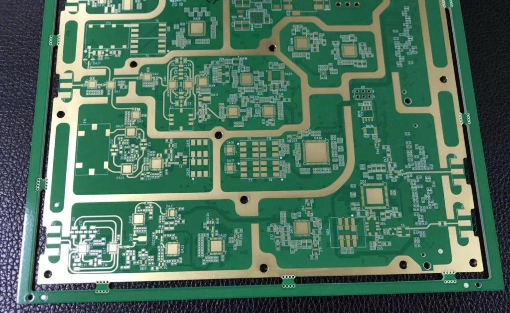
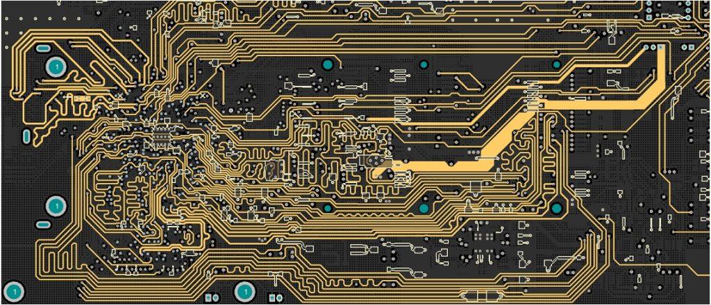
With the rapid development of the modern electronics industry, digital and high-frequency circuits are developing in the direction of high speed, low power consumption, small size, and high immunity to interference, which places higher requirements on PCB (printed circuit board) design. The Protel 99SE design system takes full advantage of the Windows XP and Windows 2000 platforms, and the great design environment of its core PCB module makes the design work more effective in achieving its design requirements. For those engaged in high-frequency circuit design, it is no longer a simple requirement for the PCB cloth through rate but requires designers to have solid theoretical knowledge and extensive experience in PCB design based on the operational characteristics of the circuit and the actual working environment to consider its design, only then we can produce the ideal PCB.
This article addresses the layout of high-frequency circuits in the PCB design process, wiring two aspects, Protel 99SE software as an example, to discuss the countermeasures and design techniques for high-frequency circuits in the PCB design process.
A high-frequency PCB layout
Layout operation is very important in the entire PCB design. The layout is the basis for wiring operations. To achieve the perfect layout of components, designers need to think about the layout of components from the perspective of the circuit’s working characteristics and alignment.
Protel 99SE has the function of automatic layout, with the clustered and statistical layout of two functions, but it does not fully meet the functional requirements of high-frequency circuits; designers also need to consider the layout from the PCB’s manufacturability, mechanical structure, heat dissipation, EMI (electromagnetic interference), reliability, signal integrity, Etc. This way, it can improve the life of the PCB, stability, and EMC (electromagnetic compatibility) to make the layout perfect.
For the layout of high-frequency circuits, designers should first consider the layout of those components that are closely matched to the structure and fixed position (such as power sockets, indicators, connectors and switches, Etc.), followed by the layout of special components on the line (such as heating elements, transformers, chips, Etc.), and finally the layout of some small devices. At the same time, to consider the wiring requirements, high-frequency components should be placed as compact as possible, and the signal line wiring should be as short as possible to reduce the crosstalk of signal lines as much as possible.
1, mechanical structure
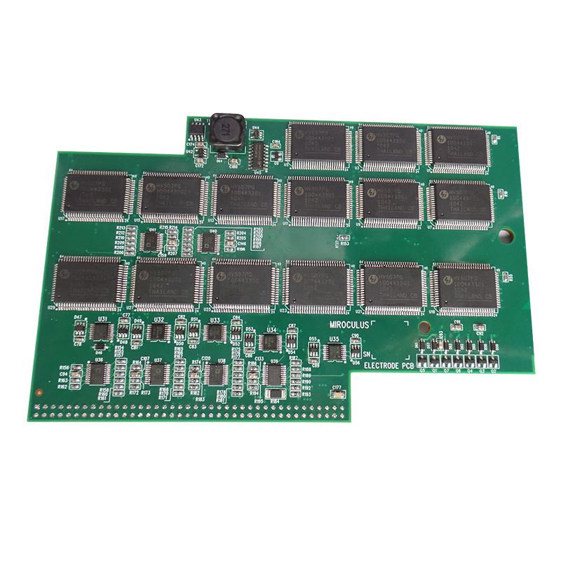
Power sockets, indicators, connectors and switches belong to this type of component and are related to the mechanical side of the positioning plug-ins. Usually, the interface between the power supply and the PCB is placed at the edge of the PCB, and the edge of the PCB to the distance is generally not less than 2mm; indicating that light-emitting diodes should be placed as needed; switches and some fine-tuning components, such as adjustable inductors, adjustable resistors, Etc. should be placed close to the edge of the PCB to facilitate adjustment and connection; components that need to be replaced frequently must be placed in the location of the device is relatively small to be easily replaced. Components with a mass of more than 15g should be fixed with a bracket, and large and heavy components should not be placed directly onto the PCB.
2, thermal aspects
High-power tubes, transformers, rectifiers and other heat-generating devices working in the high-frequency state generate more heat, in the layout should be fully considered ventilation and heat dissipation; such components are placed on the edge of the PCB or ventilation, vertical board, heat-generating components should be placed on the upper part of the board, the bottom of the double panel shall not be placed on the heat-generating components. High-power rectifier tubes, adjusting tubes, Etc., should be equipped with heat sinks and be away from the transformer. Electrolytic capacitors and other components afraid of heat should also be far away from the heat-generating devices. Otherwise, the electrolyte will be baked dry, causing its resistance to increase, causing performance deterioration, and affecting the stability of the circuit.
3, the layout of special components
As the power supply device will generate a 50Hz leakage magnetic field inside, it will interfere with the low-frequency amplifier when it is interconnected with some parts of the low-frequency amplifier. Therefore, they must be isolated or shielded.
It is best to arrange all amplifier levels in a straight line according to the schematic diagram. The advantage of such an arrangement is that the ground current of all levels will flow in this closed stage without affecting the work of other circuits. The input stage and output stage should be as far away as possible to reduce the parasitic coupling interference between them. Low-frequency circuits should be separated from high-frequency circuits, and analogue circuits from digital circuits. Integrated circuits should be placed in the centre of the PCB so that the pins are easily connected to the wiring of other devices.
Inductors, transformers and other devices have magnetic coupling and should be placed orthogonally to reduce magnetic coupling. In addition, they have a strong magnetic field; there should be an appropriately large space around them or magnetic shielding to reduce the impact on other circuits.
4, electromagnetic interference
We commonly used to eliminate electromagnetic interference methods to reduce the loop, filtering, shielding, minimize the speed of high-frequency devices, increase the dielectric constant of the PCB and other methods.
Such integrated circuit decoupling capacitors should be placed as close as possible, generally operating frequency below 10MHz with 0.1uF capacitor and 10MHz above the 0.01uF capacitor.
Some components or wires have a high potential difference between them; the distance should be increased to avoid discharge. Components with high voltage should be arranged in places that are not easily accessible by hand during debugging. Easy to interfere with each other’s components and can not be too close; input and output components should be as far away as possible to avoid feedback interference. High-frequency components to reduce the distribution parameters, generally placed near (irregular arrangement) general circuit (low-frequency circuit), should be arranged according to the rules to facilitate welding installation.
Second, high-frequency PCB wiring.
High-frequency circuits tend to be more integrated, wiring density, the use of a multi-layer board is necessary for wiring is also an effective means of reducing interference; Protel 99SE PCB system can provide 32 signal layers, 16 mechanical layers, as well as anti-solder layer, solder paste layer, more than 70 working layers for the user to choose. Reasonable choice of layers can significantly reduce the size of the PCB, can make full use of the middle layer to set up shielding, can be better achieved near the ground, can effectively reduce parasitic inductance, can effectively shorten the signal transmission length, can significantly reduce the crosstalk between signals. All these are beneficial to the reliability of high-frequency circuit work; some information shows that for the same material, a four-layer board, the double-sided noise is 20dB lower, but the higher the number of layers, the more complex the manufacturing process, and the higher the cost.
1, general wiring principles
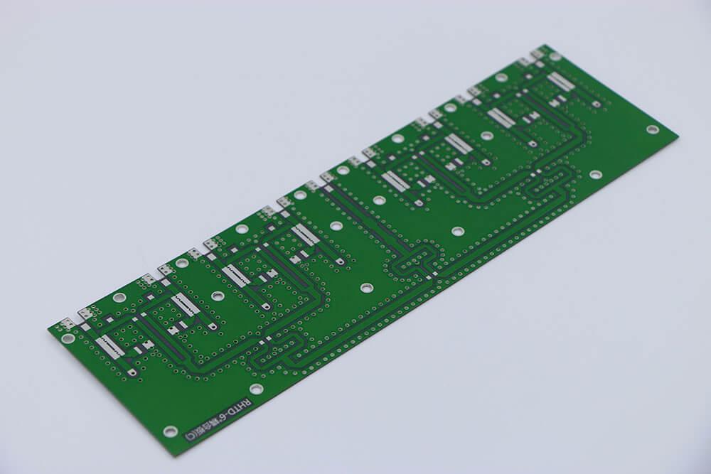
The shorter the wire between the pins of high-frequency circuit devices, the better, and the fewer bends, the better; the wire is best to use a full straight line and should try to avoid sharp bends and sharp corners; the need to turn, the application of arcs or folding line transition. This requirement in the low-frequency circuit is only used to improve the steel foil bonding strength. In contrast, in the high-frequency circuit, meeting this requirement can reduce the external emission of high-frequency signals and coupling between each other. High-frequency circuit wiring in the adjacent layers is best to take the horizontal and vertical wiring alternately; the same layer of parallel alignment can not be avoided but can be laid in a large area on the reverse side of the PCB to reduce interference for the commonly used double-sided, the multi-layer board can be used in the middle of the power layer to achieve this function.
2, power lines and ground wiring
Multi-level circuit to prevent local current ground resistance interference, all levels of the circuit should be grounded separately a short (or try to focus on grounding), the high-frequency circuit in the 3 0 M H z above, then use a large area ground. The internal components at all levels should also focus on a small ground area. Susceptible to interference devices and lines available in the ground surround, all types of signal alignment can not form a loop, the ground line can not form a current loop, and power lines and ground should be close to minimize the area enclosed out to reduce electromagnetic interference. In the wiring, the width of the wire is between 12-80mil, the power line is generally taken 20mil-40mil, and the ground line is generally taken 40mil or more, and in the case possible, the wire is as wide as possible.
Analogue ground, digital ground, Etc. Connected to the common ground to use a high-frequency choke link; in the current assembly, a high-frequency choke link is often used in the centre hole through the wire high-frequency ferrite beads, but in the circuit schematic on it is generally not expressed; the formation of the network table does not contain such components, the wiring will therefore ignore its existence, for this reality, it can be treated as an inductor in the schematic, in the PCB In response to this reality, it can be treated as an inductor in the schematic diagram. A separate component package is defined for it in the PCB component library, and it is manually moved to a suitable location near the common ground convergence point before wiring.
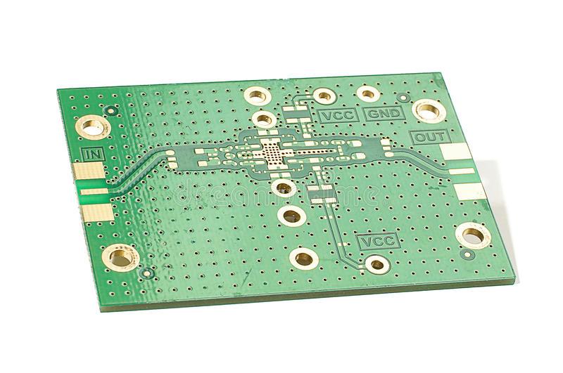
3, wiring of integrated chips
A high-frequency decoupling capacitor should be set near each integrated circuit block because Protel 99SE software does not consider the position of the decoupling capacitor and the decoupled integrated circuit when automatically placing the components left to the software, so the two are too far apart, the decoupling effect is not good, it is necessary to manually move the components to intervene in advance in the location of the two so that they are close to each other.
4、Copper laying
The main purpose of copper laying is to improve the circuit’s anti-interference ability; At the same time, the PCB heat dissipation and PCB strength are greatly beneficial, and copper laying ground can play a shielding role. However, can not use a large area strip of copper foil because the use of PCB time is too long and will generate greater heat when the strip of copper foil is prone to expansion and shedding phenomenon; therefore, in the copper laying, the best use of grid-like copper foil, and this grid and the circuit grounding network connected so that the grid will have a better shielding effect, the size of the grid network by the interference frequency to be focused on shielding.
Third, concluding remarks.
The High-frequency circuit PCB design process is complex, in addition to the design countermeasures discussed above, including signal crosstalk, signal integrity, how to suppress noise and other issues. Hence, the designer needs to have comprehensive planning and consideration in the design of the various stages of the design cycle using different methods of technology to ensure the accuracy of the design to design a good, high-frequency PCB with excellent performance.
Anpllopcb providing some of the most innovative printed circuit board technologies and highest quality standards in the industry. You can count on us to meet your needs, from the simplest boards to the most complex designs for small quantity and large scale production.

