- FPCB technology trends
- FPCB’s main raw materials
- FPCB manufacturing process
- Means of preparing flexible circuits
- Single-layer FPCB production 18 steps
- FPCB’s future innovation direction
- Conclusion
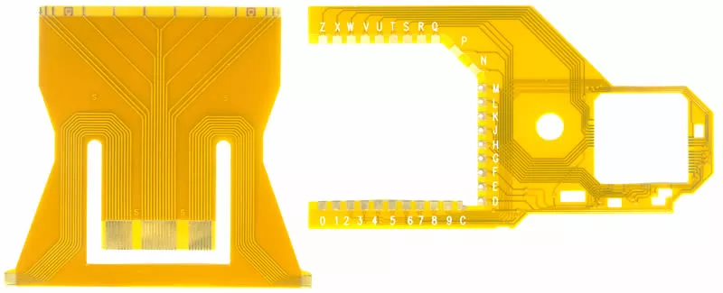
Introduction: FPCB, also known as the flexible circuit board, has the characteristics of being foldable, bendable, lightweight, small in size, and have good heat dissipation, but FPCB is slightly lacking in component carrying capacity, the good thing is that this is made up in the design of soft and hard structures. The use of FPCB has largely reduced the size of electronic products, in line with the needs of electronic products for high density, miniaturization, and high-reliability direction.
FPCB technology trends
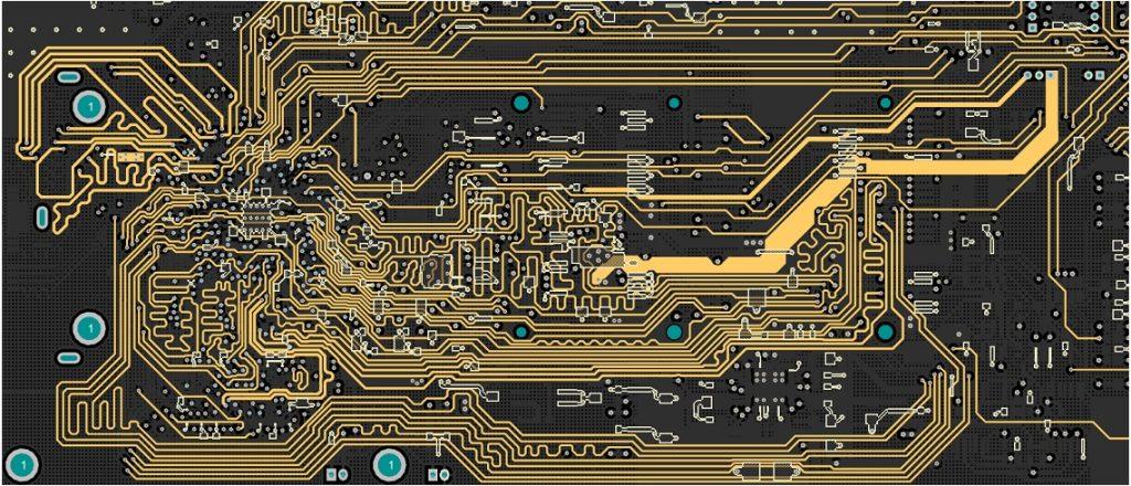
With the diversification of uses and pocket size, FPCB used in electronic devices require high-density circuitry and high performance in a qualitative sense. Recent changes in FPCB circuit density. Single-sided circuits with a conductor pitch of 30um or less can be formed by the reduction method (etching method), and double-sided circuits with a conductor pitch of 50um or less have also become practical. The conductor hole diameter between the conductor layers connecting double-sided or multilayer circuits is also becoming smaller. The conductor hole diameter of 100um or less has reached the mass production scale.
The range of possible manufacturing of high-density circuits is based on the position of manufacturing master technology. Based on circuit pitch and via aperture diameter, high-density circuits are broadly classified into three types:
- conventional FPCB,
- high-density FPCB
- ultra-high-density FPCB
The conventional reduced-form method has mass-produced FPCB with a pitch of 150 um and a lead-through aperture of 15 um. Due to the improvement of materials or processing devices, it is possible to process line pitches of 30 um even in the reduced-form method. In addition, the introduction of processes such as CO2 laser or chemical etching has made it possible to process 50um vias in mass production. Most high-density FPCB in mass production are now processed using these technologies.
However, suppose the pitch is below 25um, and the aperture diameter is below 50um. In that case, even if the traditional technology is improved, it isn’t easy to improve the qualification rate, and new processes or materials must be introduced. Various processing methods are proposed now, but the semi-additive method using electroforming (sputtering) technology is the most applicable method, and not only the basic process is different, but also the materials and auxiliary materials used are different.
On the other hand, advances in FPCB bonding technology require FPCB with higher reliability performance. With the high density of circuits, the performance of FPCB has raised diverse and high-performance requirements, largely dependent on the circuit processing technology or the materials used.
FPCB‘s main raw materials
The main raw materials: 1, substrate; 2, cover film; 3, reinforcement; and 4, other auxiliary materials.
1、Substrate material
1.1 Adhesive substrate
There are three main parts of adhesive substrate: copper foil, adhesive, and PI, two categories of the single-sided substrate and double-sided substrate, the material with only one side of copper foil is the single-sided substrate, the material with two sides of copper foil is the double-sided substrate.
1.2 Non-adhesive substrates
It has the advantages of being thinner, better dimensional stability, higher heat resistance, higher bending resistance, and better chemical resistance than glued substrates, and it is now widely used.
Copper foil: At present, the commonly used copper foil thickness has the following specifications, 1OZ, 1/2OZ, 1/3OZ, now the introduction of 1/4OZ thickness of thinner copper foil, but the current domestic use of such materials, in doing ultra-fine road (line width line distance of 0.05MM and below) products. With customers’ increasing requirements, this kind of specification material will be widely used in the future.
2、Covering film
There are mainly three parts: release paper, glue, and PI; the final retention of the product is only two parts of glue and PI; the release paper will be torn off in the production process and no longer used (its role is to protect the glue on foreign objects).
3、Tonic
For FPCB-specific use of materials in a specific part of the product to increase the support strength, to make up for the FPCB “soft” characteristics.
At present, the commonly used reinforcement materials are as follows.
▶ FR4 reinforcement: the main components are glass fiber cloth and epoxy resin adhesive, the same as the FR4 material used in PCB.
▶ Steel reinforcement: The steel composition has strong hardness and support strength.
▶ PI reinforcement: the same as the cover film, consisting of PI and adhesive release paper, except that the PI layer is thicker and can be produced in ratios from 2MIL to 9MIL.
4、Other auxiliary materials
▶Pure adhesive: This adhesive film is a heat-curing acrylic adhesive film with a protective paper/release film and a layer of the adhesive composition, mainly used for laminate, soft and hard combination board, and FR-4/steel reinforcement board, which play a bonding role.
▶ Electromagnetic protection film: Paste on the board surface to play a shielding role.
▶Pure copper foil: consisting of only copper foil, mainly used for hollow board production.
FPCB manufacturing process
The FPCB manufacturing process so far has almost always been processed using the reduced-form method (etching method). Usually, the copper-clad foil board is used as the starting material, the resist layer is formed by the photolithography method, and the circuit conductor is formed by etching to remove the unwanted part of the copper surface. Due to problems such as side etching, the etching method has limitations for processing microfine circuits.
Based on the processing difficulties of the subtractive method or the difficulty of maintaining high-yield microfabrication, the semi-additive method was considered effective, and various semi-additive solutions were proposed.
Examples of microfabrication using the semi-additive method. The semi-addition process uses a polyimide film as the starting material and first casts (coats) a liquid polyimide resin on a suitable carrier to form a polyimide film. Then, the sputtering method forms a crystal implantation layer on the polyimide substrate film. Then, a resist layer pattern, called a plating-resistant layer, is formed on the crystal implantation layer using the photolithography method to form the inverse pattern of the circuit.
The conductor circuit is formed by plating on the blank part. Then, the resist layer and the unnecessary implant layer are removed to form the first circuit layer. A photosensitive polyimide resin is coated on the first circuit layer to form a hole using photolithography, a protective layer, or an insulating layer for the second circuit layer. A crystal implant layer is sputtered on it to form a substrate conductive layer for the second circuit layer. Repeating the above process, multilayer circuits can be formed.
Using this semi-addition method, it is possible to process ultra-fine circuits with a pitch of 5um and a conductive hole of towel 10um. The key to making ultra-fine circuits by the semi-addition method is the performance of the photosensitive polyimide resin used as an insulating layer.
Means of preparing flexible circuits
Any device with flexibility can be called a flexible electronic device, and the materials associated with it can also be called flexible electronic materials. Flexible electronics can be said to be through screen printing, ink jet printing, electrostatic spinning, transfer embossing, and other certain processes to achieve organic or inorganic electronic materials or devices made to a flexible substrate in the device substrate can withstand the deformation range, maintaining the same performance is called flexible electronics. And the general method to achieve flexible electronics: is through the flexible material itself to make flexible devices; through transfer printing technology, the use of silicon and other hard film strips in the flexible soft substrate to form a periodic sinusoidal curve to obtain flexibility; according to the island bridge structure, with bendable wires to connect the microelectronics to obtain flexibility; the use of open grid structure, the silicon-based semiconductor film itself designed into an open grid structure and obtained flexibility, Etc.
Soft etching method
Soft etching is a general term for micro-contact printing technology, nanoimprinting technology, soft molding technology, solvent-assisted micro-molding, Etc. It provides a simple, effective, low-cost way to fabricate microns and nanopatterns on flat, curved surfaces. Micro-contact printing, mainly for structurally simple patterns, can be prepared on a large scale demand. The basic principle is to use elastic templates combined with self-assembled single molecular layer technology to print graphics on substrates. Nanoimprinting, a technique that uses a rigid template instead of an elastic template for imprinting, consists of two steps: elastic template imprinting and pattern transfer (or residual photoresist removal). A substrate is coated with a layer of polymer so that a rigid plate with a target nanogram is engraved, and the polymer coating of the substrate is embossed at a temperature higher than the polymer’s glass transition to form the target pattern. The hard plate is then removed to obtain the nanopattern.
Laser-directed sintering method.
The graphene oxide is first coated on the surface of the DVD. After the graphene oxide forms a thin film on the surface of the disc, a laser path is designed to make a directional sintering laser motion on the DVD, allowing the high temperature of the laser to reduce the graphene oxide under the path, which leads to the formation of conductive reduced graphene (r-GO) and finally the formation of reduced graphene flexible circuits.
AgNWs/PDMS method
The AgNWs slurry is prepared by screen printing, and the circuit structure to be prepared is printed on the clean glass substrate surface. Then the AgNWs conductive network structure pattern is obtained by vacuum baking at 150°C, heating for one hour, and thoroughly removing the organic solvent from the slurry. Then the freshly prepared liquid PDMS solution is poured on the surface of the printed pattern. After the PDMS solution fully enters the gaps of the AgNWs conductive network, the PDMS is cured by heating at a low temperature for 4h at 60°C. Finally, the whole structure is peeled off from the surface of the glass substrate, and a stretchable circuit structure is obtained.
Ag fiber method
The template method is a synthesis method to construct effective and adjustable morphology, structure, and size of the synthesized nanomaterials with the template as the main body, which can affect the material properties. In the fabrication of Ag fiber flexible circuits, Ag fibers are prepared by the template method and then placed in an agate mortar and ground sufficiently for 4-8h. Then the mixed organic solvent is added to the milled Ag fiber and milled to obtain the formulated Ag fiber with the slurry of mixed organic solvent. Finally, this Ag fiber/mixed organic solvent slurry is processed by printing circuits on PET flexible substrates using screen printing technology. A low temperature of 300°C is provided during this process. Finally, Ag fiber flexible circuits can be prepared.
Screen printing
Screen printing has the advantages of simple equipment, easy operation, easy and low-cost printing and plate making, and high adaptability, and it is widely used in the electronics field. In flexible circuits, screen templates are made from screens with different mesh sizes, and then the screens are stretched using wooden or iron rigid frames to hold the screens around. Generally, the substrate is attached to a rigid surface, and the patterned screen template is attached to the flexible substrate. Then the prepared conductive ink is applied to the screen pattern, thus forming a conductive pattern to produce a flexible circuit.
Inkjet Printing Patterning
Inkjet printing uses conductive ink, which is printed into circuit patterns with the help of an inkjet printer. Conductive substances such as silver nanoparticles are commonly used to make inks of suitable density and viscosity. The circuit patterns are printed on the flexible substrate with the help of the printer to prepare flexible circuits.
Single-layer FPCB production 18 steps
Step 1: Cut copper laminate by size
Step 2: Micro-etching to remove the oxidation of the copper foil surface and add copper plating.
Step 3: punching holes
Step 4: blackening: make the non-conductive part of the hole wall conductive in preparation for subsequent copper plating.
Step 5: Copper plating, so the upper and lower copper surface is conductive.
Step 6: Apply dry film – make dry/wet photosensitive film and copper surface.
Step 7: exposure – (similar to the photo), there are positive and negative films; the positive film is through the film exposure part of the reaction, not the exposed part.
Step 8: Development – through the development solution, remove the dry film that does not react part.
Step 9: etching – remove the copper not protected by the dry film so that the line left is the dry film + copper two-layer structure.
Step 10: Peel off the dry film – the dry film will be removed to reveal the copper line.
Step 11: AOI inspection (Automatic Optical Inspection)
Step 12: Apply protective film
Step 13: Solder Resist Ink Printing
Step 14: Exposure will reveal the area where the window is needed; the photoresist ink is negative, and the principle is the same as in step 7.
Step 15: Baking hardening
Step 16: Gold plating to protect the line
Step 17: Text printing
Step 18: Other subsequent cutting and other processes
FPCB‘s future innovation direction
FPCB should be continuously innovated from three aspects, mainly in.
1, thickness: the thickness of the FPCB must be more flexible, need to do more thin.
2, folding resistance: The inherent characteristics of FPCB can be bent, so the future FPCB folding resistance must be stronger.
3, process level: to meet the requirements of many aspects, the FPCB process must be upgraded, and the minimum aperture and line width/line spacing must meet higher requirements.
Conclusion
You have already understood the manufacturing process and procedures of FPCB; Anpllopcb provides the best flexible PCB manufacturing services to suit your preferences. You can contact us with details of your requirements, and we will get back to you as soon as possible.


